978-1-4673-8888-7/16/$31.00 ©2016 IEEE
Space Vector Modulation for Three-Level NPC
Inverter Using Two-Level Space Vector Diagram
Narendra Babu A
Department of Electrical Engineering
Indian Institute of Technology Roorkee
Roorkee,Uttarakhand, India
narendra7iitr@gmail.com
Pramod Agarwal
Department of Electrical Engineering
Indian Institute of Technology Roorkee
Roorkee Uttarakhand, India
pramgfee@iitr.ac.in
Abstract— A novel concept that uses two-level (2L) space
vector diagram (SVD) to achieve three-level (3L) space vector
modulation (SVM) is introduced in this paper. Main emphasis
is given on neutral-point (NP) clamped (NPC) inverter, though,
the idea does not depend on the topology. Two interesting
schemes for NPC namely nearest three vector (N3V)
modulation and nearest three virtual vector (N3VV)
modulation are considered for detailed analysis. The main
technical drawback of NP voltage oscillations with N3V is a
effectively addressed by N3VV for full modulation and power
factor range. However, the extensive calculations involved in
the process of obtaining the duty ratios have made this method
difficult to implement. In this paper, first, simple mathematical
relations are established for N3V and N3VV modulation
methods using 2L SVM. Later, appropriate modulation
algorithms are developed for implementation. The simplicity of
the proposed modulation approach has a significant impact on
execution process. No simplifications have made in the Space
vector diagram (SVD) unlike some newly proposed simplified
schemes. The performance of the proposed modulation
algorithm is simulated in MATLAB, Simulink for various
operating conditions.
Keywords—
Neutral point clamped (NPC) inverter, Virtual
vectors (VV), Space vector modulation (SVM)
I.
I
NTRODUCTION
In neutral point (NP) clamped (NPC) inverter with single
DC-source, flow of neutral current develops a voltage ripple
in the neutral point (NP) depending on the operating point.
As derived in [1], the ripple is negligible for UPF and is
more significant when the power factor decreases. This NP
voltage oscillations will cause overvoltage stress on the
devices lead to failure, decrease the output wave shape
quality (even order harmonics for unequal capacitor
voltages) and reduction of maximum switching frequency
[2],etc.
The nearest three vector (N3V) is a widely used PWM
technique for multilevel inverters in digital environment
[3][4][5]. However, in NPC, it is not possible to attain a zero
averaged NP current in each switching period by using N3V
for entire modulation index and power factors range. The
drawback is eliminated by using an interesting non-nearest
three vector (non-N3V) modulation scheme known as
nearest three virtual vector (N3VV) PWM [6], which can
eliminate NP voltage ripple for all power factors in the linear
modulation range. However, due to inequality of sub-triangle
regions in the space vector diagram (SVD) of these non-
NTV methods, the calculation of duty ratios is quit complex.
Some authors used phase duty ratios to simplify the
computations, yet requires closed loop correction [6].
Another approach is to neglect some least significant
switching states to simplify SVD is presented in [7]. Others
[8] have limitation in the modulation index.
The aim of this study is to establish various duty ratio
expressions of N3V and N3VV in terms of an equivalent 2L
SVM formed by outer most voltage vectors. Later, with the
help of 2L duty ratios, an algorithm is developed for 3L NPC
inverter. No simplifications made to actual three level (3L)
space vector diagram (SVD) and can be calculated
completely online.
(1)
2
DC
V
+
0
P
i
1
C
1C
V
2C
V
2
C
abc
i
a
b
c
NP
1a
S
2a
S
2b
S
1b
S
1
c
S
2c
S
1a
S
1c
S
1b
S
2b
S
2c
S
2a
S
(2)
C
V
N
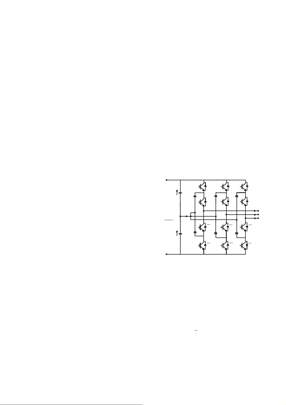
Fig. 1. Circuit schematic of three-level NPC inverter
II. S
PACE
V
ECTOR
D
IAGRAM AND
D
UTY RATION
EXPRESSIONS
Fig.1 shows the power circuit of 3L NPC operating with
single DC-source. Taking
N
as reference, the switching
table and corresponding output voltages are given in the
Table I. The aim of the converter is to synthesize the three
phase reference voltages at the ac side collectively
represented as a space vector given by
j2 /3 j4 /3
ab c
2
.( . . )
3
ref
Vvveve
ππ
=+ +
(1)


