DDR5 SPD规格:JEDEC JESD400-5详解
"JEDEC JESD400-5标准详细定义了DDR5内存模块的串行存在检测(SPD)内容。该文档旨在提供关于内存通道上所有模块的关键信息,供系统的BIOS用于正确初始化和优化系统内存。DDR5 SPD非易失性存储器的容量在标准中有所规定。"
DDR5 Serial Presence Detect (SPD) 是DDR5内存技术中的一个重要组成部分,它是一种存储关键信息的小型非易失性存储器,位于内存模块上。JEDEC(Joint Electron Device Engineering Council,联合电子设备工程委员会)是制定半导体行业标准的组织,JESD400-5是JEDEC发布的关于DDR5 SPD的规范。
在DDR5内存系统中,SPD数据包含了关于内存模块的多个方面信息,如内存的类型、速度、电压等级、时序设置、散热信息、制造商信息等。这些数据对于系统BIOS来说至关重要,因为它们需要这些信息来识别并配置内存条,确保系统的稳定运行和性能优化。与DDR4相比,DDR5 SPD引入了更多的特性以支持更高的内存带宽、更低的功耗和更先进的功能。
DDR5 SPD的一个显著改进是其容量的增加。由于DDR5内存模块的技术升级,SPD需要存储更多数据以适应新的特性和功能,比如动态电压和频率调整(DVFS)、电源管理设置、多列数据包处理(Multi-Rank Interleaving)等。这使得DDR5 SPD能够支持更复杂的系统配置和未来扩展。
此外,DDR5 SPD还引入了更快速的通信协议,使用了更高速的I2C接口,以满足更快的数据传输需求。这个接口允许系统更快地读取SPD信息,从而加快系统的启动时间和配置过程。
JEDEC标准的制定遵循严格的程序,包括董事局级别的审查和法律顾问的确认。这些标准的目的是为了消除制造商和购买者之间的误解,促进产品的互换性和改进,帮助购买者迅速选择并获取合适的内存产品,无论是在国内还是国际市场。
需要注意的是,JEDEC标准的制定不考虑是否涉及专利,也不承担任何专利所有者的责任,或对采用JEDEC标准的各方有任何义务。这意味着标准的使用者需要自行解决可能存在的知识产权问题。
JESD400-5 DDR5 SPD标准详细定义了内存模块的配置信息,为系统提供了自动识别和优化内存性能的依据,同时也反映了DDR5技术在性能、效率和扩展性方面的进步。
JEDEC Standard No. 400-5
Page 6
4.6 NVDIMM-N Overlay Schema
Key Byte 2 contains value 0x12 (DDR5)
Key Byte 3 contains any of the following values:
• 0x9X, NVDIMM-N Hybrid
where X refers to the base memory architecture
4.7 NVDIMM-P Overlay Schema
Key Byte 2 contains value 0x12 (DDR5)
Key Byte 3 contains any of the following values:
• 0xAX, NVDIMM-P Hybrid
where X refers to the base memory architecture
After programming the SPD contents, suppliers of JEDEC compliant modules must set the write protect bits for SPD
device blocks 0 through 7. See JESD300-5 SPD5118 Device Specification for details on the Write Protect command
protocol.
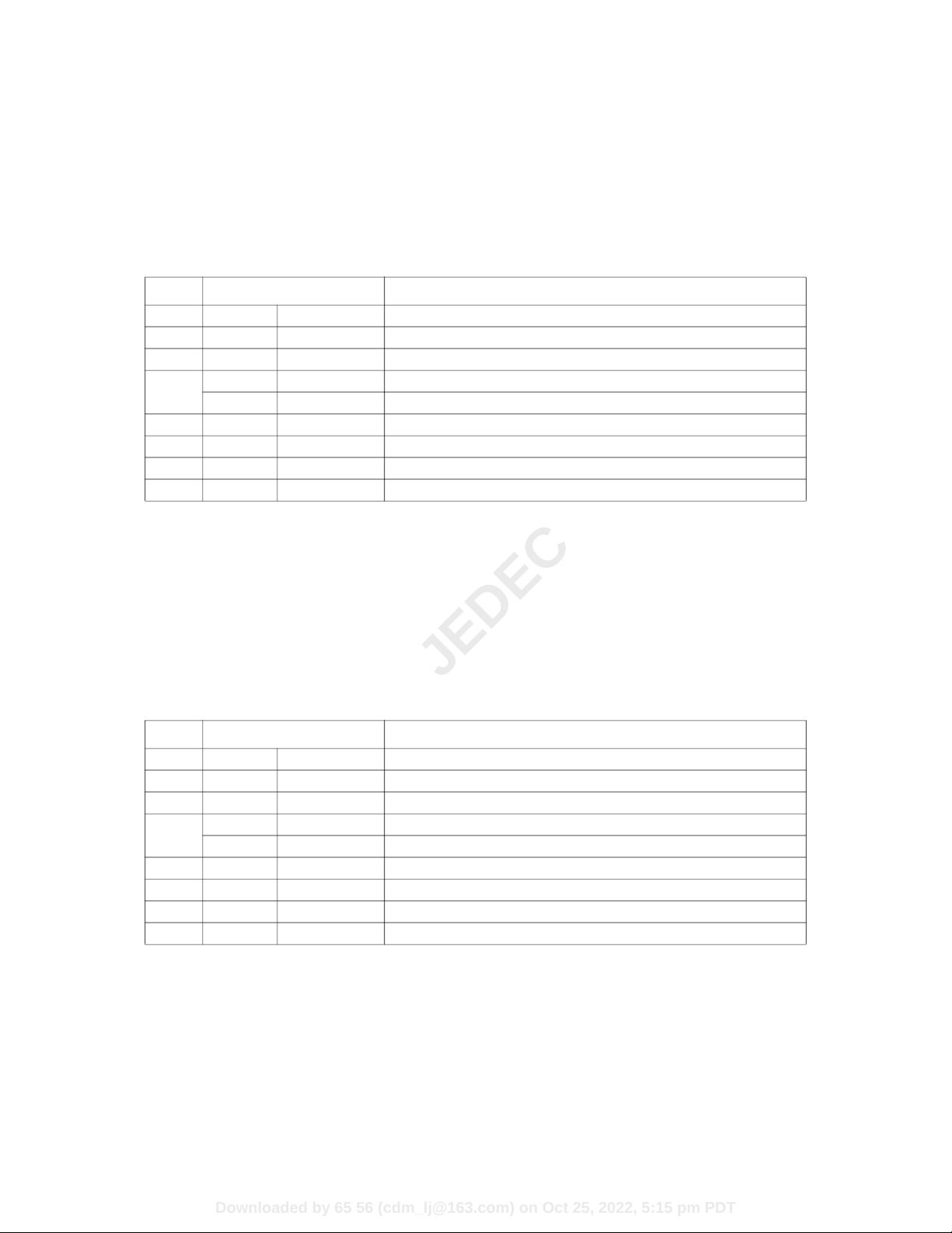
Block Range Description
0 0~63 0x000~0x03F Base Configuration and DRAM Parameters
1 64~127 0x040~0x07F Base Configuration and DRAM Parameters
2 128~191 0x080~0x0BF ...
3
192~239 0x0C0~0x0EF Insert Annex A.0: Common
240~255 0x0D0~0x0FF Insert Annex A.6: NVDIMM-N Memory Module Types
4 256~319 0x100~0x13F Insert Annex A.6: NVDIMM-N Memory Module Types
5 320~383 0x140~0x17F Insert Annex A.6: NVDIMM-N Memory Module Types
6 384~447 0x180~0x1BF Insert Annex A.6: NVDIMM-N Memory Module Types
7~15 448~1023 0x180~0x3FF ...
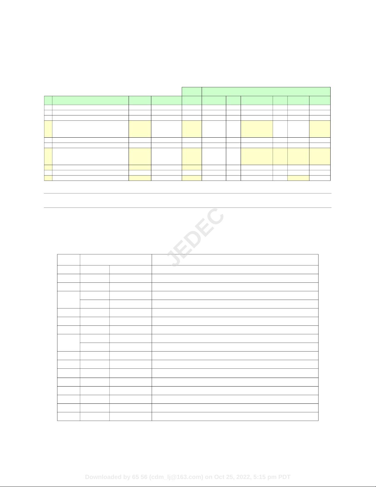
Block Range Description
0 0~63 0x000~0x03F Base Configuration and DRAM Parameters
1 64~127 0x040~0x07F Base Configuration and DRAM Parameters
2 128~191 0x080~0x0BF ...
3
192~239 0x0C0~0x0EF Insert Annex A.0: Common
240~255 0x0D0~0x0FF Insert Annex A.7: NVDIMM-P Memory Module Types
4 256~319 0x100~0x13F Insert Annex A.7: NVDIMM-P Memory Module Types
5 320~383 0x140~0x17F Insert Annex A.7: NVDIMM-P Memory Module Types
6 384~447 0x180~0x1BF Insert Annex A.7: NVDIMM-P Memory Module Types
7~15 448~1023 0x180~0x3FF ...
Downloaded by 65 56 (cdm_lj@163.com) on Oct 25, 2022, 5:15 pm PDT
JEDEC

剩余108页未读,继续阅读
点击了解资源详情
点击了解资源详情
点击了解资源详情
2023-11-07 上传
2023-05-23 上传
点击了解资源详情
点击了解资源详情
2022-11-28 上传
2021-10-01 上传

Gabriel_fei
- 粉丝: 1
- 资源: 31
 我的内容管理
展开
我的内容管理
展开


最新资源
- CoreOS部署神器:configdrive_creator脚本详解
- 探索CCR-Studio.github.io: JavaScript的前沿实践平台
- RapidMatter:Web企业架构设计即服务应用平台
- 电影数据整合:ETL过程与数据库加载实现
- R语言文本分析工作坊资源库详细介绍
- QML小程序实现风车旋转动画教程
- Magento小部件字段验证扩展功能实现
- Flutter入门项目:my_stock应用程序开发指南
- React项目引导:快速构建、测试与部署
- 利用物联网智能技术提升设备安全
- 软件工程师校招笔试题-编程面试大学完整学习计划
- Node.js跨平台JavaScript运行时环境介绍
- 使用护照js和Google Outh的身份验证器教程
- PHP基础教程:掌握PHP编程语言
- Wheel:Vim/Neovim高效缓冲区管理与导航插件
- 在英特尔NUC5i5RYK上安装并优化Kodi运行环境
