Abstract— An 840-GHz Schottky diode detector is
integrated with an analog lock-in amplifier in 130-nm bulk
CMOS. The integrated lock-in amplifier can support a
modulation frequency of up to 10MHz with a gain of 54dB, a
dynamic range of 42dB, and an input referred noise of less
than 10
at modulation frequencies higher than
100kHz. The integrated lock-in amplifier occupies an area of
0.17 mm
2
and consumes 4.9mA from a 1.2-V supply. The
detector and on-chip lock-in amplifier combination was used
to form terahertz images.
Index Terms—Terahertz, imaging, Schottky barrier diode,
lock-in amplifier, quadrature
I. INTRODUCTION
Numerous terahertz (THz) detectors and detector arrays
in CMOS for imaging applications have been reported [1]-
[4]. These circuits were characterized using an external
lock-in amplifier (LIA). This has limited practical
realization of an imager as well as an imaging array that
can output signals from a column of detectors for higher
frame rate imaging. This paper reports an 840-GHz
Schottky barrier Diode (SBD) [1] imaging pixel that
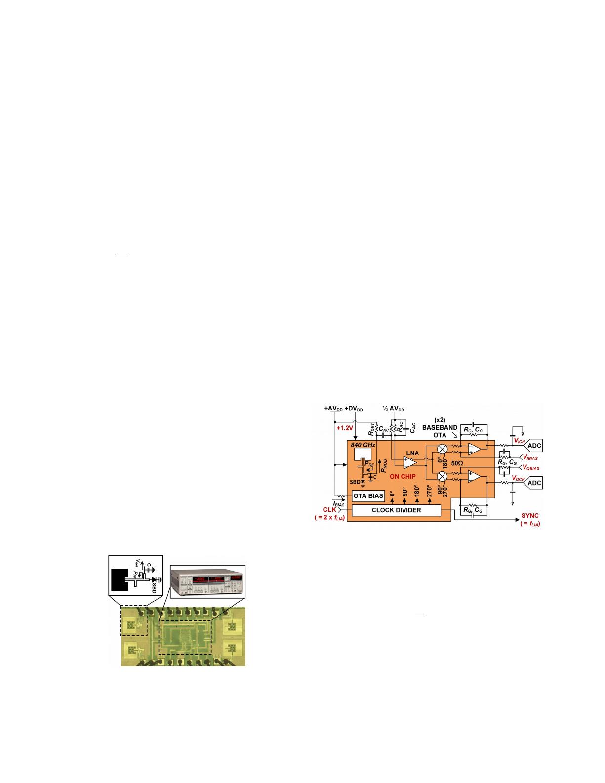
incorporates a wideband on-chip LIA (Fig. 1).
The modulation frequency bandwidth of 10MHz was
chosen in order to mitigate the impact of flicker noise
present in detectors. This bandwidth is 10X higher than
that of the previously reported integrated LIA [5] and
~100X higher than that of an instrumentation LIA
(Stanford Research model SR810 [6]). The noise
performance of the on-chip LIA is also comparable to that
of the SR810.
Fig. 1. (Top Left) 840GHz antenna and detector. (Top Right)
SR810 LIA [6]. (Bottom) THz imaging pixel with an on-chip
LIA.
II. THEORY OF OPERATION AND DESIGN
An LIA is a homodyne receiver that uses a local
oscillator signal
followed by low-pass filters (LPF's)
that determine the noise filtering property of the LIA. An
LIA can also incorporate a quadrature channel to enable
measurements of both amplitude and phase of the detected
signal. The LPF's are used to reject the majority of the
mixed AC components, especially the
component
and the noise. The LIA step response time is inversely
related to the 3-dB bandwidth of the LPF, and there is a
trade-off between SNR and response time [6].
An LIA and four 840-GHz detectors, including those
that utilize a Schottky diode, were integrated in foundry
130-nm CMOS. Implementation of the Schottky diode
detectors does not require any process modifications [1].
A block diagram of the LIA and a single 840-GHz SBD
pixel when configured for imaging is illustrated in Fig. 2.
Fig. 2. Chip block diagram configured for imaging.
A. Detectors
The SBD detector used for imaging is shown in Fig. 1.
The detector is composed of four 0.4x0.4µm
2
Schottky
diode cells connected in parallel [1]. The detector
achieves a responsivity of 273 V/W and a noise-equivalent
power (NEP) of 42
at 860GHz and modulation
frequency of 1MHz. The SBD is forward biased at 20µA
using an off-chip resistor (R
DET
= 41kΩ). The output of the
detector is then brought to an off-chip AC coupling
network to bias the low-noise preamplifier (LNA) inputs
at a common-mode voltage of +600mV.
[1][2][3][4]
0.84-THz Imaging Pixel with a Lock-in Amplifier in CMOS
Rui Xu
1
, Ja-Yol Lee
2
, Dae Yeon Kim
1
, Shinwoong Park
3
, Zeshan Ahmad
1
, Kenneth K. O.
1
1
Texas Analog Center of Excellence and Dept. of EE, U. of Texas at Dallas, USA
2
RF SoC Research Section, Electronics and Telecommunications Research Institute, S. Korea
3
RFIC Lab, Multifunctional Integrated Circuits & Systems Group, Virginia Tech, USA
rayxu123@gmail.com
978-1-4673-8651-7/16/$31.00 © 2016 IEEE 2016 IEEE Radio Frequency Integrated Circuits Symposium
RMO3A-3
166


