"TI-MSP430FE427.pdf 数据手册及产品样本"
下载需积分: 9 | PDF格式 | 1.53MB |
更新于2024-01-18
| 68 浏览量 | 举报
通过阅读TI-MSP430FE427.pdf,我们可以了解到该产品是一款高性能微控制器,属于Texas Instruments(TI)公司的MSP430系列。该系列是一种低功耗、高性能的16位超低功耗MCU,适用于各种应用,例如智能电网、消费电子产品以及医疗器械等。
TI-MSP430FE427.pdf提供了该产品的详细技术规格和功能介绍。首先,该微控制器采用了16位的RISC体系结构,在低频操作下具有出色的性能和低功耗。它内置了16KB的闪存和256字节的RAM,可以存储大量的程序代码和数据。此外,该微控制器还支持多种外设接口,如UART、SPI和I2C等,方便与其他设备进行通信。
TI-MSP430FE427.pdf还详细介绍了该产品的功耗特性。该微控制器通过优化电源管理技术,实现了低功耗运行。在最低功耗模式下,仅需几个微安的电流就可以维持系统运行,大大延长了电池寿命。这使得TI-MSP430FE427在无线传感器网络、移动设备等对电池寿命要求高的应用场景中具有很大的优势。
此外,TI-MSP430FE427.pdf还介绍了该产品的可靠性和安全性。该微控制器采用了机械、热和电气等多种保护机制,确保了系统在各种恶劣环境下的可靠性。同时,它还支持硬件加密和运行时编译,保护了应用程序的安全性,防止被非法攻击和篡改。
TI-MSP430FE427.pdf提供了该产品的开发工具和支持资源。TI公司提供了一整套的软件开发工具包,包括IDE、编译器和调试器等,方便开发人员进行软件开发和调试。此外,TI还提供了丰富的技术资料和应用案例,帮助开发者快速上手和解决问题。
总体而言,TI-MSP430FE427是一款高性能、低功耗、可靠安全的16位微控制器。该产品适用于各种应用,可以满足物联网、智能家居、工业自动化等多个领域的需求。TI公司提供了全面的技术支持和资源,帮助开发者快速开发应用,提高产品竞争力。
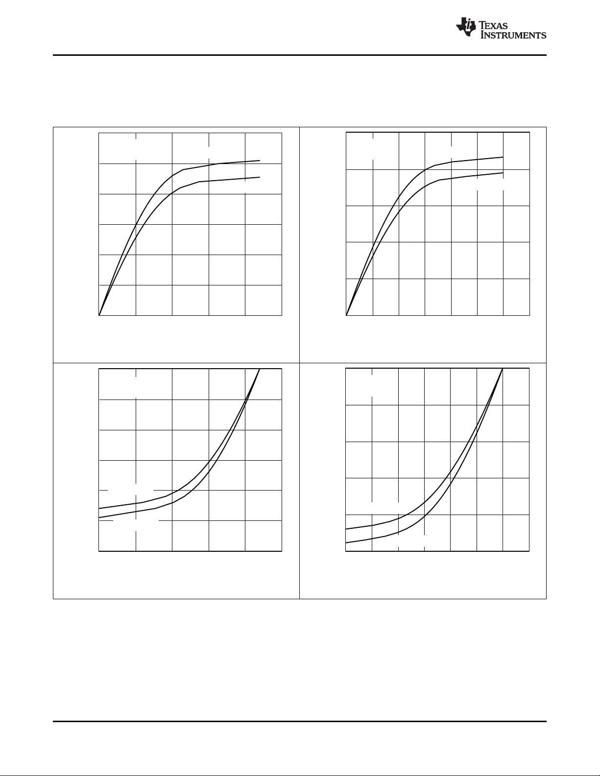
Frequency
1.8 V 3.6 V
2.7 V 3 V
4.15 MHz
8.4 MHz
V − Supply Voltage − V
CC
f − Maximum Processor Frequency − MHz
System
Supply voltage range with
ESP430 or SD16 enabled and during
programming of the flash memory
Supply voltage range
during program execution
6 MHz
11
MSP430FE427, MSP430FE425, MSP430FE423
www.ti.com
SLAS396D –JULY 2003–REVISED NOVEMBER 2016
Submit Documentation Feedback
Product Folder Links: MSP430FE427 MSP430FE425 MSP430FE423
SpecificationsCopyright © 2003–2016, Texas Instruments Incorporated
Figure 5-1. Frequency vs Supply Voltage
(1) All inputs are tied to 0 V or V
CC
. Outputs do not source or sink any current. The current consumption in LPM2, LPM3, and LPM4 are
measured with active Basic Timer1 and LCD (ACLK selected). The current consumption of the ESP430CE1 and the SVS module are
specified in their respective sections. LPMx currents measured with WDT+ disabled. The currents are characterized with a KDS
Daishinku DT−38 (6 pF) crystal.
(2) Current consumption for brownout is included.
5.4 Supply Current Into AV
CC
and DV
CC
Excluding External Current
(1)
over recommended operating free-air temperature range (unless otherwise noted)
PARAMETER T
A
V
CC
MIN TYP MAX UNIT
I
(AM)
Active mode (AM)
f
(MCLK)
= f
(SMCLK)
= f
(DCO)
= 1 MHz,
f
(ACLK)
= 32768 Hz, XTS_FLL = 0,
program executes in flash
–40°C to 85°C 3 V 400 500 µA
I
(LPM0)
Low-power mode 0 or 1 (LPM0 or LPM1)
(2)
f
(MCLK)
= f
(SMCLK)
= f
(DCO)
= 1 MHz,
f
(ACLK)
= 32768 Hz, XTS_FLL = 0,
FN_8 = FN_4 = FN_3 = FN_2 = 0
–40°C to 85°C 3 V 130 150 µA
I
(LPM2)
Low-power mode 2 (LPM2)
(2)
–40°C to 85°C 3 V 10 22 µA
I
(LPM3)
Low-power mode 3 (LPM3)
(2)
–40°C
3 V
1.5 2.0
µA
25°C 1.6 2.1
60°C 1.7 2.2
85°C 2.0 3.5
I
(LPM4)
Low-power mode 4 (LPM4)
(2)
–40°C
3 V
0.1 0.5
µA25°C 0.1 0.5
85°C 0.8 2.5
Current consumption of active mode versus system frequency:
I
(AM)
= I
(AM)
[1 MHz] × f
(System)
[MHz]
Current consumption of active mode versus supply voltage:
I
(AM)
= I
(AM)
[3 V] + 170 µA/V × (V
CC
– 3 V)
剩余65页未读,继续阅读
相关推荐


不觉明了
- 粉丝: 8601
 我的内容管理
展开
我的内容管理
展开


最新资源
- 易语言实现标签云特效的源码教程
- SpringBoot与Kafka集成入门教程
- Delphi文本资料分类管理程序源码发布
- ABB PLC AC500 CM574-RS 操作文档详解
- 全面解读nmon数据监控与报表分析技术
- Java入门基础教程完整版
- 年度总结汇报必备:10大PPT实用插件推荐
- STM32硬件调试:ISP程序下载与Flash烧写教程
- 易语言实现画板图片左右滚动效果源码分析
- JQuery表单验证插件EasyValidator使用教程
- Java程序员入职指南:职业规划清晰解读
- 深入浅出Android架构层次与核心技术要点
- 易语言进阶教程:实现画板模拟打印预览功能
- EKF室内定位技术:Android平台的WiFi追踪实现
- 掌握DIV+CSS布局,快速入门指南
- MySQL 5.7.x 监控脚本:自定义监控与脚本入门
