"TI-SN75DP119.pdf:高效DP中继器产品样本"
需积分: 10 69 浏览量
更新于2024-01-22
4
收藏 2.06MB PDF 举报
"TI-SN75DP119.pdf"是一份关于DP中继器的产品规格说明书。该产品是一种用于DisplayPort(DP)连接中继的芯片,可以在不同设备之间传输高清视频和音频信号。这份规格说明书详细介绍了该中继器的技术参数、功能特点、应用范围和性能参数。
首先,规格说明书简要介绍了DP中继器的工作原理和应用场景。DP中继器是一种用于延长DP信号传输距离的器件,通常用于连接笔记本电脑、台式机、显示器、投影仪等设备之间。它能够支持高达4K分辨率的视频传输,以及高保真的音频传输,使得用户能够在不同设备之间实现高清视频和音频的传输和共享。
其次,规格说明书详细介绍了TI-SN75DP119中继器的技术参数和功能特点。该中继器采用了先进的DP技术,支持DP 1.4标准,具有高达8 Gbps的数据传输速率,以及高达32通道的音频传输能力。此外,该中继器还支持HDCP 2.2加密协议,能够有效保护高清内容的传输安全。除此之外,规格说明书还介绍了中继器的接口类型、供电方式、工作温度范围等技术参数,为用户提供了全面的技术信息。
除了技术参数外,规格说明书还介绍了TI-SN75DP119中继器的性能参数和应用范围。该中继器具有卓越的传输稳定性和通用性,能够在各种显示设备和音频设备中实现高清视频和音频的传输。它可以广泛应用于电脑办公、娱乐媒体、数字家庭影院等领域,为用户提供了高品质的视频和音频体验。
最后,规格说明书还介绍了TI-SN75DP119中继器的安装和使用方法,以及注意事项和维护保养说明。该中继器采用了简易的连接方式,用户只需将其插入设备的DP接口即可实现信号传输。规格说明书还提供了详细的安装步骤和使用说明,以及常见故障处理和维护保养的注意事项,方便用户进行操作和维护。
总的来说,"TI-SN75DP119.pdf"是一份详细且全面的产品规格说明书,为用户提供了关于DP中继器的技术参数、功能特点、性能参数、应用范围、安装使用方法和注意事项等方面的全面信息。该规格说明书具有很高的参考价值,可供用户在购买、安装和使用DP中继器时进行参考和指导。
SN75DP119
SLLSE12A –NOVEMBER 2009–REVISED JULY 2014
www.ti.com
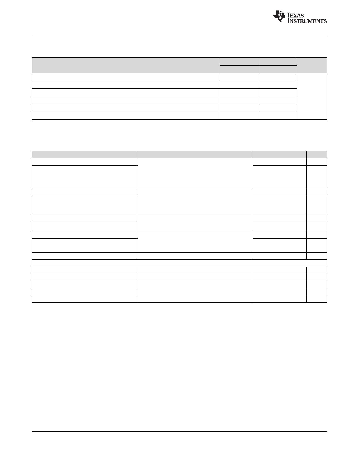
7.4 Thermal Information
RGY RHH
THERMAL METRIC
(1)
UNIT
14 PINS 36 PINS
R
θJA
Junction-to-ambient thermal resistance 45 34
R
θJC(top)
Junction-to-case (top) thermal resistance 20 20
R
θJB
Junction-to-board thermal resistance 16 17
°C/W
ψ
JT
Junction-to-top characterization parameter n/a n/a
ψ
JB
Junction-to-board characterization parameter n/a n/a
R
θJC(bot)
Junction-to-case (bottom) thermal resistance 12 12
(1) For more information about traditional and new thermal metrics, see the IC Package Thermal Metrics application report, SPRA953.
7.5 Electrical Characteristics
over recommended operating conditions (unless otherwise noted)
PARAMETER TEST CONDITIONS MIN TYP MAX UNIT
I
CCDP1max
Supply current 1 DP lane selected WorstCase: 16.2 21.3 mA
EN = V
CC
/2 (1-lane) or V
CC
(2-lane selected);
2.7Gbps PRBS; V
ID
= 400 mV
PP
; V
OD
= 300 mVpp,
8.5 dB pre-emp (PRE_CTL=V
CC
; V
O
D_CTL=GND);
I
CCDP2max
Supply current 2 DP lanes selected 31.7 41.4 mA
EQ_CTL = V
CC
(6 dB); V
CC
= 3.3 V (for typ) and
V
CC
= 3.6 V (for max),
(1)
I
CCDP3max
Supply current 1 DP lane selected EN = V
CC
/2 (1-lane) or VCC (2-lane selected); 12.9 17.6 mA
2.7Gbps PRBS; V
ID
= 400 mV
PP
; V
OD
= 300 mV
PP
,
0 dB pre-emp (PRE_CTL = GND); VOD_CTL = VCC/2);
I
CCDP4max
Supply current 2 DP lanes selected 24.9 34.1 mA
EQ_CTL=GND (0 dB); V
CC
= 3.3 V (for typ) and
V
CC
= 3.6 V (for max),
I
CCDP1typ
Supply current 1 DP lane selected EN = V
CC
/2 (1-lane) or V
CC
(2-lane selected); 14.5 mA
2.7Gbps PRBS; IN/OUT; V
ID
= 600 mV
PP
; (PRE_CTL=GND);
I
CCDP2typ
Supply current 2 DP lanes selected 28.2 mA
VOD_CTL = V
CC
); V
CC
= 3.3 V, EQ_CTL = GND (no EQ)
(2)
I
CCDP3typ
Supply current 1 DP lane selected EN = V
CC
/2 (1-lane) or V
CC
(2-lane selected); 14.5 mA
2.7Gbps PRBS; no pre-emp; IN/OUT; V
ID
= 800 mV
PP
;
(PRE_CTL= VOD_CTL = V
CC
); V
CC
= 3.3 V, EQ_CT L =
I
CCDP4typ
Supply current 2 DP lanes selected 28.2 mA
GND (no EQ)
(3)
IPWRDN Shutdown current (PWRDN mode) EN = GND; 25 100 µA
3-LEVEL CONTROL PINS (EN, VOD_CTL, PRE_CTL, EQ_CTL)
I
L
Low-level input current V
I
= 0.5 V; V
CC
= 3.6 V –30 30 µA
I
H
High-level input current V
I
= V
CC
– 0.5 V; Vcc = 3.6V –30 30 µA
I
M
Mid-level input current V
I
= V
CC
/2 – 0.3V and V
I
= V
CC
/2 + 0.3 V; V
CC
= 3.6 V –30 30 µA
R
bias
Input bias resistance See Figure 6 105 125 145 kΩ
R
ESD
input series resistance to biasing network See Figure 6 2 2.4 kΩ
(1) This current consumption also applies to VOD = 400mV with 5.5 dB pre-emphasis or VOD = 600mV output swing and 2dB pre-
emphasis
(2) This current consumption also applies to VOD = 300mV with 2 dB pre-emphasis
(3) This current consumption also applies to VOD = 300mV with 6dB pre-emphasis or VOD = 400mV output swing and 3.5dB pre-emphasis
6 Submit Documentation Feedback Copyright © 2009–2014, Texas Instruments Incorporated
Product Folder Links: SN75DP119
剩余28页未读,继续阅读
2023-02-07 上传
2023-02-07 上传
2023-02-07 上传
2023-02-07 上传
2023-02-07 上传
2023-02-07 上传
2023-02-07 上传
2023-02-07 上传

不觉明了
- 粉丝: 4227
- 资源: 5759
 我的内容管理
展开
我的内容管理
展开


最新资源
- 深入浅出:自定义 Grunt 任务的实践指南
- 网络物理突变工具的多点路径规划实现与分析
- multifeed: 实现多作者间的超核心共享与同步技术
- C++商品交易系统实习项目详细要求
- macOS系统Python模块whl包安装教程
- 掌握fullstackJS:构建React框架与快速开发应用
- React-Purify: 实现React组件纯净方法的工具介绍
- deck.js:构建现代HTML演示的JavaScript库
- nunn:现代C++17实现的机器学习库开源项目
- Python安装包 Acquisition-4.12-cp35-cp35m-win_amd64.whl.zip 使用说明
- Amaranthus-tuberculatus基因组分析脚本集
- Ubuntu 12.04下Realtek RTL8821AE驱动的向后移植指南
- 掌握Jest环境下的最新jsdom功能
- CAGI Toolkit:开源Asterisk PBX的AGI应用开发
- MyDropDemo: 体验QGraphicsView的拖放功能
- 远程FPGA平台上的Quartus II17.1 LCD色块闪烁现象解析
