Revision:
Prepared by:
00
Markus Hermwille
Key Words: IGBT driver, gate resistor, selection, design, application
Principles and Applications
1 / 10
2007-11-12 – Rev00
© by SEMIKRON
Introduction.............................................................................................................................................................................1
IGBT Switching Behaviour......................................................................................................................................................2
Switching Behaviour of Free-Wheeling Diode ........................................................................................................................4
Driving Output Stage ..............................................................................................................................................................4
Gate Resistor Dimensioning...................................................................................................................................................5
Minimum Gate Resistance – Maximum Gate Peak Current ...................................................................................................6
Power Dissipation...................................................................................................................................................................6
Peak Power Capability ...........................................................................................................................................................7
Resistor Type .........................................................................................................................................................................7
Design and Layout .................................................................................................................................................................7
Troubleshooting......................................................................................................................................................................9
Symbols and Terms Used ......................................................................................................................................................9
References...........................................................................................................................................................................10
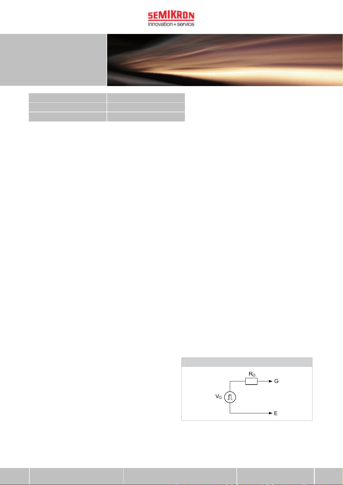
This application note provides information on the use of
gate resistors (R
G
) to control IGBT switching. The
information given in this application note contains tips
only and does not constitute complete design rules; the
information is not exhaustive. The responsibility for
proper design remains with the user.
Introduction
The switching behaviour of power semiconductors is
controlled by the gate capacitance recharge. This gate
capacitance recharge may be controlled via a gate
resistor. By using a typical positive control voltage (V
G(on)
)
of +15V the IGBT is turned-on and turned-off at a
negative output voltage (V
G(off)
) of typically -5 …-8…-15V.
The dynamic IGBT performance can be adjusted by the
value of the gate resistor.
The gate resistor influences the IGBT switching time,
switching losses, reverse bias safe operating area
(RBSOA), short-circuit safe operating area (SCSOA),
EMI, dv/dt, di/dt and reverse recovery current of the free-
wheeling diode. It has to be selected and optimized very
carefully in accordance with the individual application
parameters, e.g. IGBT technology, diode, switching
frequency, losses, application layout, inductivity / stray
inductance, DC-link voltage and driver capability. The
complete design of an application must be viewed as a
whole, with due considering of the above-mentioned
parameters. Interactive effects within the whole
application must be evaluated and accommodated.
Control by Resistance
www.Semikron.com/Application


