
August 10, 2010 / Vol. 8, No. 8 / CHINESE OPTICS LETTERS 757
Sub-nanosecond silicon-on-insulator optical micro-ring
switch with low crosstalk
Xi Xiao ( FFF)
∗
, Haihua Xu (MMM°°°uuu), Liang Zhou (±±± ), Zhiyong Li (ooo]]]),
Yuntao Li (ooo$$$777), Yude Yu (|||), and Jinzhong Yu ({{{777¥¥¥)
State Key Laboratory on Integrated Optoelectronics, Institute of Semiconductors,
Chinese Academy of Sciences, Beijing 100083, China
∗
E-mail: xixiao@semi.ac.cn
Received March 3, 2010
We demonstrate a sub-nanosecond electro-optical switch with low crosstalk in a silicon-on-insulator (SOI)
dual-coupled micro-ring embedded with p-i-n diodes. A crosstalk of –23 dB is obtained in the 20-µm-radius
micro-ring with the well-designing asymmetric dual-coupling structure. By optimizations of the doping
profiles and the fabrication processes, the sub-nanosecond switch-on/off time of < 400 ps is finally realized
under an electrical pre-emphasized driving signal. This compact and fast-response micro-ring switch, which
can be fabricated by complementary metal oxide semiconductor (CMOS) compatible technologies, have
enormous p otential in optical interconnects of multicore networks-on-chip.
OCIS co des: 130.3120, 250.6715, 230.5750, 230.4000.
doi: 10.3788/COL20100808.0757.
The rapid development of silicon photonics, including
modulators, switches, and Ge-on-Si photodetectors, has
indicated the feasibility of on-chip optical intercon-
nects in multicore computing systems. Significant in-
crements of computation performance can be exp ected if
high-data-rate optical signals can be switched with low
power. A silicon-based micro-resonator has been consid-
ered as the key component for the optical networks-on-
chip for its compactness, wavelength selectivity, and low
power consumption
[1−4]
. Some studies on silicon micro-
resonator-based optical switches have been reported,
aiming at on-chip multiplexing/demultiplexing and rout-
ing of wavelength division multiplexing signals with low
power and large bandwidth
[5−9]
. However, most of the
reported crosstalks and switch times are not sufficient
for future fast on-chip optical switching with transmis-
sion bit rates exceeding 10 Gb/s. A compact and low
crosstalk silicon-based electro-optical switch operating in
the sub-nanosecond regime remains to be demonstrated
for on-chip optical interconnects.
In this letter, we demonstrate a 1×2 silicon-on-
insulator (SOI) based micro-ring switch with low
crosstalk and sub-nanosecond switch time. The switch
crosstalk of –23 dB is obtained with the optimized asym-
metric dual-coupling micro-ring. Through the lateral
p-i-n diodes integrated to the ring waveguide, carrier-
induced plasma dispersion effect
[10]
is utilized to fast-
switch the resonance of the micro-ring. An electrical
pre-emphasized driving signal is generated and employed
for switch speed acceleration. A sub-nanosecond switch-
on/off time of 300/380 ps is realized.
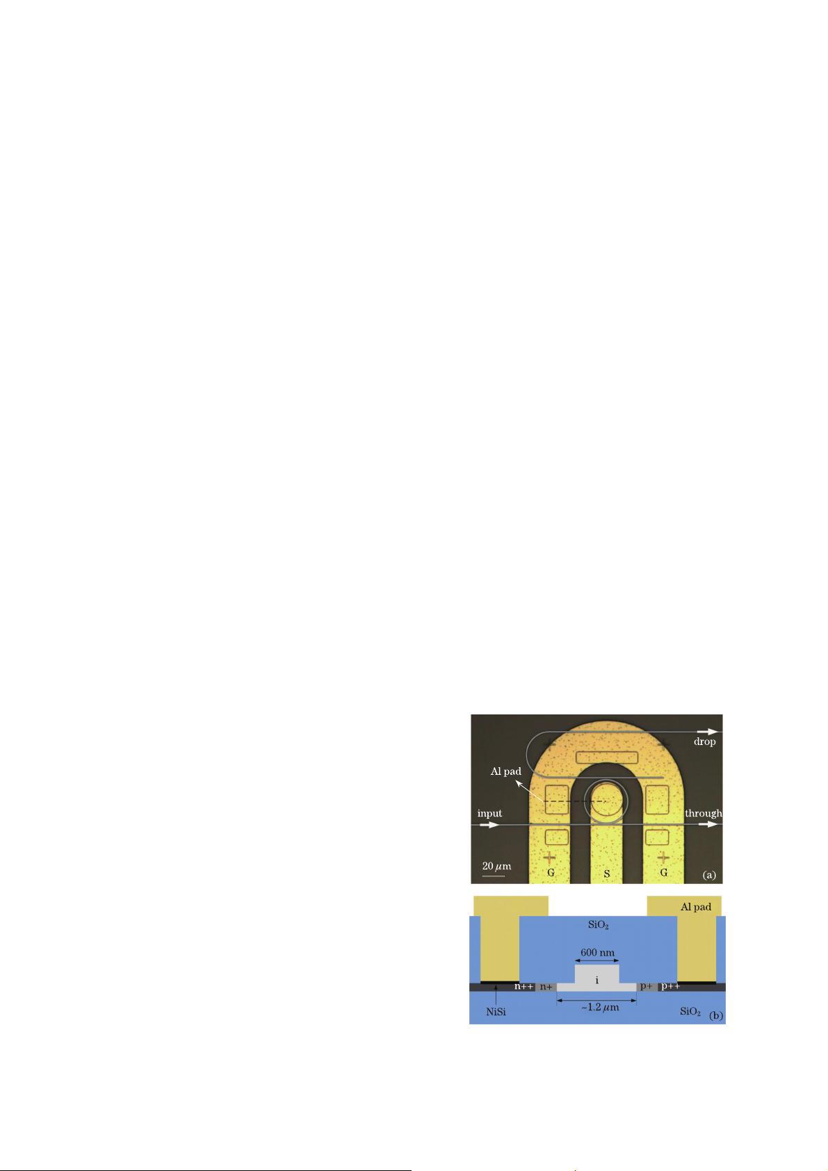
The switch consists of a 20-µm-radius dual-coupling
micro-ring surrounded by p+ and n+ doped regions.
Figure 1(a) is the top-view microscope image of the fabri-
cated switch with Al electrodes. The gray lines highlight
the 20-µm-radius micro-ring and the coupling waveg-
uides. Under forward bias, the embedded p-i-n diodes
inject the carriers into the intrinsic waveguide. The vari-
ation of the carrier density changes the refractive index
and absorption coefficient because of the plasma disper-
sion effect in silicon
[10]
. In this way, the driving electrical
signal shifts the micro-ring resonance and controls the
on/off state of the optical signals produced from the
through- and drop-ports.
Figure 1(b) shows the cross-sectional schematic of the
micro-ring waveguide and the integrated lateral p-i-n
diodes. The waveguide was fabricated on a SOI wafer
with a 340-nm top silicon layer. All the waveguides have
∼100 nm slab thickness for the electrical integration and
are single mode rib waveguides designed for transverse
electric (TE) mode transmission. The operation speed
of a forward p-i-n diode is significantly dependent on
the carrier transport distance across the waveguide
[11,12]
;
Fig. 1. (a) Top-view microscope image of the micro-ring
switch; (b) cross-section schematic of the fabricated ring
waveguide integrated with forward p-i-n diodes.
1671-7694/2010/080757-04
c
° 2010 Chinese Optics Letters
下载后可阅读完整内容,剩余3页未读,立即下载

weixin_38682161
- 粉丝: 3
- 资源: 972
 我的内容管理
展开
我的内容管理
展开


最新资源
- OptiX传输试题与SDH基础知识
- C++Builder函数详解与应用
- Linux shell (bash) 文件与字符串比较运算符详解
- Adam Gawne-Cain解读英文版WKT格式与常见投影标准
- dos命令详解:基础操作与网络测试必备
- Windows 蓝屏代码解析与处理指南
- PSoC CY8C24533在电动自行车控制器设计中的应用
- PHP整合FCKeditor网页编辑器教程
- Java Swing计算器源码示例:初学者入门教程
- Eclipse平台上的可视化开发:使用VEP与SWT
- 软件工程CASE工具实践指南
- AIX LVM详解:网络存储架构与管理
- 递归算法解析:文件系统、XML与树图
- 使用Struts2与MySQL构建Web登录验证教程
- PHP5 CLI模式:用PHP编写Shell脚本教程
- MyBatis与Spring完美整合:1.0.0-RC3详解
资源上传下载、课程学习等过程中有任何疑问或建议,欢迎提出宝贵意见哦~我们会及时处理!
点击此处反馈


