NOIP1SN5000A, NOIP1SN2000A
www.onsemi.com
15
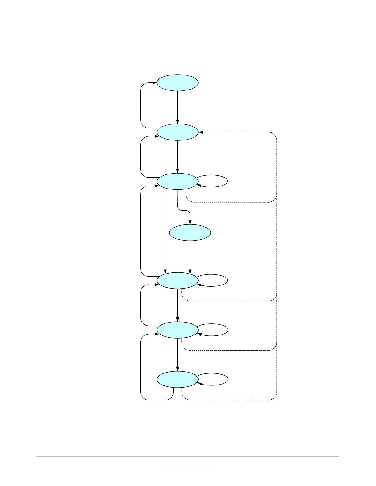
Sensor States
Low Power Standby
In low power standby state, all power supplies are on, but
internally every block is disabled. No internal clock is
running (PLL / LVDS clock receiver is disabled).
All register settings are set to their default values (see
Table 35).
Only a subset of the SPI registers is active for read/write
in order to be able to configure clock settings and leave the
low power standby state. The only SPI registers that should
be touched are the ones required for the ‘Enable Clock
Management’ action described in Enable Clock
Management − Part 1 on page 16
Standby (1)
In standby state, the PLL/LVDS clock receiver is running,
but the derived logic clock signal is not enabled.
Standby (2)
In standby state, the derived logic clock signal is running.
All SPI registers are active, meaning that all SPI registers
can be accessed for read or write operations. All other blocks
are disabled.
Idle
In the idle state, all internal blocks are enabled, except the
sequencer block. The sensor is ready to start grabbing
images as soon as the sequencer block is enabled.
Running
In running state, the sensor is enabled and grabbing
images. The sensor can be operated in global master/slave
modes.
User Actions: Power Up Functional Mode Sequences
Power Up Sequence
Figure 17 shows the power up sequence of the sensor. The
figure indicates that the first supply to ramp−up is the
vdd_18 supply, followed by vdd_33 and vdd_pix
respectively. It is important to comply with the described
sequence. Any other supply ramping sequence may lead to
high current peaks and, as consequence, a failure of the
sensor power up.
The clock input should start running when all supplies are
stabilized. When the clock frequency is stable, the reset_n
signal can be de−asserted. After a wait period of 10 ms, the
power up sequence is finished and the first SPI upload can
be initiated.
NOTE: The ‘clock input’ can be the CMOS PLL clock
input (clk_pll), or the LVDS clock input
(lvds_clock_inn/p) in case the PLL is bypassed.
Figure 17. Power Up Sequence
reset_n
vdd_18
vdd_33
clock input
vdd_pix
> 10us> 10us> 10us > 10us
SPI Upload
> 10us
Enable Clock Management − Part 1
The ‘Enable Clock Management’ action configures the
clock management blocks and activates the clock generation
and distribution circuits in a pre−defined way. First, a set of
clock settings must be uploaded through the SPI register.
These settings are dependent on the desired operation mode
of the sensor.
Table 6 shows the SPI uploads to be executed to configure
the sensor for P1−SN/SE 8−bit and 10−bit serial, with and
without the PLL.
If the PLL is not used, the LVDS clock input must be
running.
It is important to follow the upload sequence listed in
Table 6.
Use of Phase Locked Loop
If PLL is used, the PLL is started after the upload of the
SPI registers. The PLL requires (dependent on the settings)
some time to generate a stable output clock. A lock detect
circuit detects if the clock is stable. When complete, this is
flagged in a status register.
Check the PLL_lock flag 24[0] by reading the SPI
register. When the flag is set, the ‘Enable Clock
Management− Part 2’ action can be continued. When PLL
is not used, this step can be bypassed as shown in Figure 16
on page 14.


