- 17 -
datasheet LPDDR3 SDRAMK3QF2F20EM-QGCE
K3QF2F20EM-QGCF
Rev. 1.0
3.0 LPDDR3 PAD DEFINITION AND DESCRIPTION
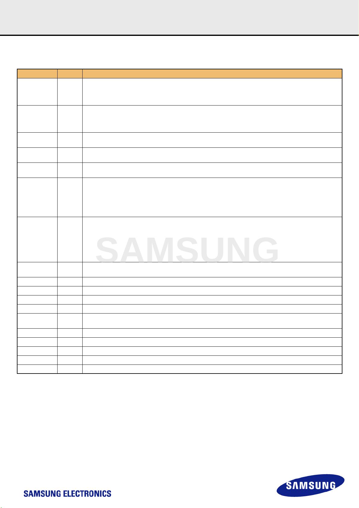
[Table 1] Pad Definition and Description
NOTE :
1) Data includes DQ and DM.
Name Type Description
CK_t, CK_c Input
Clock: CK_t and CK_c are differential clock inputs. All Double Data Rate (DDR) CA inputs are sampled on both positive
and negative edge of CK_t. Single Data Rate (SDR) inputs, CS_n and CKE, are sampled at the positive Clock edge.
Clock is defined as the differential pair, CK_t and CK_c. The positive Clock edge is defined by the crosspoint of a rising
CK_t and a falling CK_c. The negative Clock edge is defined by the cross point of a falling CK_t and a rising CK_c.
CKE0, CKE1 Input
Clock Enable: CKE HIGH activates and CKE LOW deactivates internal clock signals and therefore device input buffers
and output drivers. Power savings modes are entered and exited through CKE transitions.
CKE is considered part of the command code. See [Table 5] for command code descriptions. CKE is sampled at the positive
Clock edge.
CS0_n, CS1_n Input
Chip Select: CS_n is considered part of the command code. See [Table 5] for command code descriptions.
CS_n is sampled at the positive Clock edge.
CA0 - CA9 Input
DDR Command/Address Inputs: Uni-directional command/address bus inputs.
CA is considered part of the command code. See [Table 5] for command code descriptions.
DQ0 - DQ31
(x32)
I/O Data Inputs/Outputs: Bi-directional data bus
DQS0_t-DQS3_t
DQS0_c-DQS3_c
(x32)
I/O
Data Strobes (Bi-directional, Differential): The data strobe is bi-directional (used for read and write data) and differential
(DQS_t and DQS_c). It is output with read data and input with write data. DQS is edge-aligned to read data and centered
with write data.
For x32, DQS0_t and DQS0_c correspond to the data on DQ0 - DQ7, DQS1_t and DQS1_c to the data on DQ8 - DQ15,
DQS2_t and DQS2_c to the data on DQ16 - DQ23, DQS3_t and DQS3_c to the data on DQ24 - DQ31.
DM0 - DM3
(x32)
Input
Input Data Mask: DM is the input mask signal for write data. Input data is masked when DM is sampled HIGH coincident
with that input data during a Write access. DM is sampled on both edges of DQS. Although DM is for input only, the DM
loading shall match the DQ and DQS_t (or DQS_c).
For x32 device, DM0 is the input data mask signal for the data on DQ0-7, DM1 is the input data mask signal for the data
on DQ8-15. DM2 is the input data mask signal for the data on DQ16-23 and DM3 is the input data mask signal for the data
on DQ24-31.
ODT Input
On Die Termination: This signal enables and disables termination on the DRAM DQ bus according to the specified mode
register settings.
V
DD1
Supply Core Power Supply 1: Core power supply.
V
DD2
Supply Core Power Supply 2: Core power supply.
V
DDCA
Supply Input Receiver Power Supply: Power supply for CA0-9, CKE, CS_n, CK_t, and CK_c input buffers.
V
DDQ
Supply I/O Power Supply: Power supply for Data input/output buffers.
V
REF
(CA) Supply
Reference Voltage for CA Command and Control Input Receiver: Reference voltage for all CA0-9, CKE, CS_n, CK_t,
and CK_c input buffers.
V
REF
(DQ) Supply Reference Voltage for DQ Input Receiver: Reference voltage for all data input buffers.
V
SS
Supply Ground
V
SSCA
Supply Ground for Input Receivers
V
SSQ
Supply I/O Ground: Ground for data input/output buffers
ZQ I/O Reference Pin for Output Drive Strength Calibration
