"半导体制造工艺-刻蚀技术解析"
版权申诉
Semiconductor manufacturing has revolutionized various aspects of human life, from computing to communication, networking, aerospace, and defense technologies. Among the key processes involved in semiconductor manufacturing is etching, which plays a crucial role in transferring patterns onto silicon wafers.
Etching is the process of selectively removing material from a wafer to create patterns or structures. This is typically done by exposing the wafer to a chemical or physical reaction that removes material from unprotected areas. As semiconductor technology advances with the development of large-scale integrated circuits, the demands for finer line widths and larger wafer sizes have increased, making the etching process more critical than ever.
Understanding the fundamentals of etching is essential for anyone involved in semiconductor manufacturing. By learning about etching processes, individuals can gain insights into how patterns are created on silicon wafers, leading to the production of complex and advanced semiconductor devices.
In conclusion, etching is a fundamental process in semiconductor manufacturing that plays a crucial role in creating intricate patterns on silicon wafers. As the semiconductor industry continues to advance, the importance of etching processes will only continue to grow, making it essential for individuals to stay informed and knowledgeable about this critical aspect of semiconductor manufacturing.
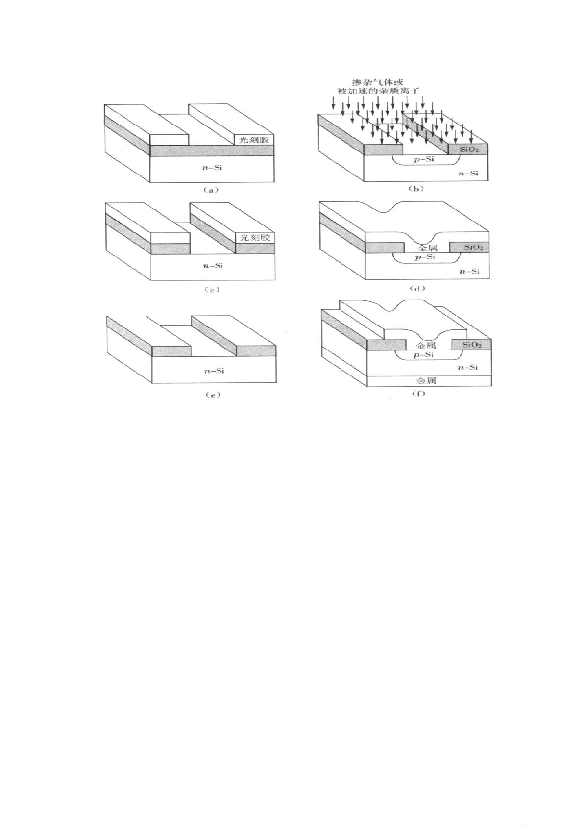
图 1-2:(a)显影后的晶片;(b)SiO
2
去除的晶片;(c)光刻工艺处理后的晶片;(d)扩散
或离子注入形成 p-n 结;(e)光刻工艺处理后的晶片;(f)完整工艺处理后的晶片
图 1-2(a)显示了显影后的晶片。晶片再次放入 120~180℃温度下烘焙 20
分钟,以增强对称底得黏附力,提高在即将进行的刻蚀工艺处理中的腐蚀能力。
然后使用氢氟酸(HF)作为酸刻蚀液来去除没有被光刻胶抗蚀剂所保护的 SiO
2
表面,如图 1-2(b)所示。最后使用化学溶剂或等离子体氧化系统剥去光刻胶。
图 1-2(c)显示光刻胶光刻胶工艺处理以后除去部分氧化层区域的最终结果,此
时晶片已经完成了准备工作,可以进行后续的扩散或离子注入的工艺步骤以形成
p-n 结。
1.3 扩散和离子注入
在扩散方法中,没有被 SiO
2
保护的半导体表面暴露在相反类型的高浓度杂
质中,杂质利用固态扩散的方法进入半导体晶格中。在离子注入方法中,掺杂离
子被加速到较高的能量,然后注入半导体内部。此时 SiO
2
层作为杂质扩散或离

剩余36页未读,继续阅读
164 浏览量
281 浏览量
2021-10-08 上传
129 浏览量
2021-10-12 上传
111 浏览量

猫一样的女子245
- 粉丝: 234
 我的内容管理
展开
我的内容管理
展开


最新资源
- 乘风多用户PHP统计系统v4.1:源码与项目实践指南
- Vue.js拖放组件:vue-smooth-dnd的封装与应用
- WPF图片浏览器开发教程与源码分享
- 泰坦尼克号获救预测:分享完整版机器学习训练测试数据
- 深入理解雅克比和高斯赛德尔迭代法在C++中的实现
- 脉冲序列调制与跳周期调制相结合的Buck变换器研究
- 探索OpenCV中的PCA人脸检测技术
- Oracle分区技术:表、索引与索引分区深入解析
- Windows 64位SVN客户端下载安装指南
- SSM与Shiro整合的实践案例分析
- 全局滑模控制Buck变换器设计及其仿真分析
- 1602液晶动态显示实现源码及使用教程下载
- Struts2、Hibernate与Spring整合在线音乐平台源码解析
- 掌握.NET Reflector 8.2.0.42:反编译及源码调试技巧
- 掌握grunt-buddha-xiaofangmoon插件的入门指南
- 定频滑模控制在Buck变换器设计中的应用
