A Whole Integrated System for Detection of Neural
Signal and Wireless Transmission
Dang Hua*, Qu Ruoyuan, Chen Zhiming, Gui Xiaoyan and Wang Xinghua
School of Information and Electronics
Beijing Institute of Technology
Beijing, China
Email: danghua@bit.edu.cn
Abstract—A whole integrated system for detection of Neural
Signal and wireless transmission at 2.4G-2.5GHz is presented in
this paper. The system is consisted of low noise OPA, high
precision analog to digital convertor (ADC), radio-frequency (RF)
transmitter and RF receiver. Analog processing module are
specially designed based on high input impedance and low noise
requirements for neural signal detection, and RF circuits are
based on IEEE STD802.15 transmitter characteristics.
Fabricated in a 0.18
m CMOS process and tested in a neural
acquisition system, the IC prototype occupies 2.88mm
2
and
works functionally, which can be a wide solution for wireless
neural signal processor.
Keywords—LNopa, ADC, wireless technique, neural signal.
I. INTRODUCTION
The biological brain and neural function research has been
more and more popular in modern medical and clinical
application: on the one hand, Electrical stimulation by neural
microelectrodes has been applied in treatment of intractable
diseases such as polio and Parkinson's disease; on the other
hand, real neural signals offers reliable data for diagnosis[1].
However, the traditional wired acquisition is inconvenient,
which not only constrains the freely moving measured object,
but also causes distraction, SNR decline and wound
infection[2]. In order to overcome all these limitations and
acquire specific electronic neural signal which is more accurate,
safer, and more efficient and less delay, this paper presents a
wireless neural acquisition system, which has been fabricated
and tested in 0.18ȣm CMOS process. The RF works on a
bandwidth of 2.4G-2.5GHz. That is because bandwidth
between 2.4G-2.4835GHz is ISM (Industrial Scientific Medical)
Band, which is license free and makes the design in this paper
usable for as many applications as possible. This paper is
organized as below: circuit design considerations will be
introduced in the second part; the chip test result will be
analyzed in the third part; the fourth part is the summary of the
main work.
II. C
IRCUIT DESIGN
A. Architecture Design
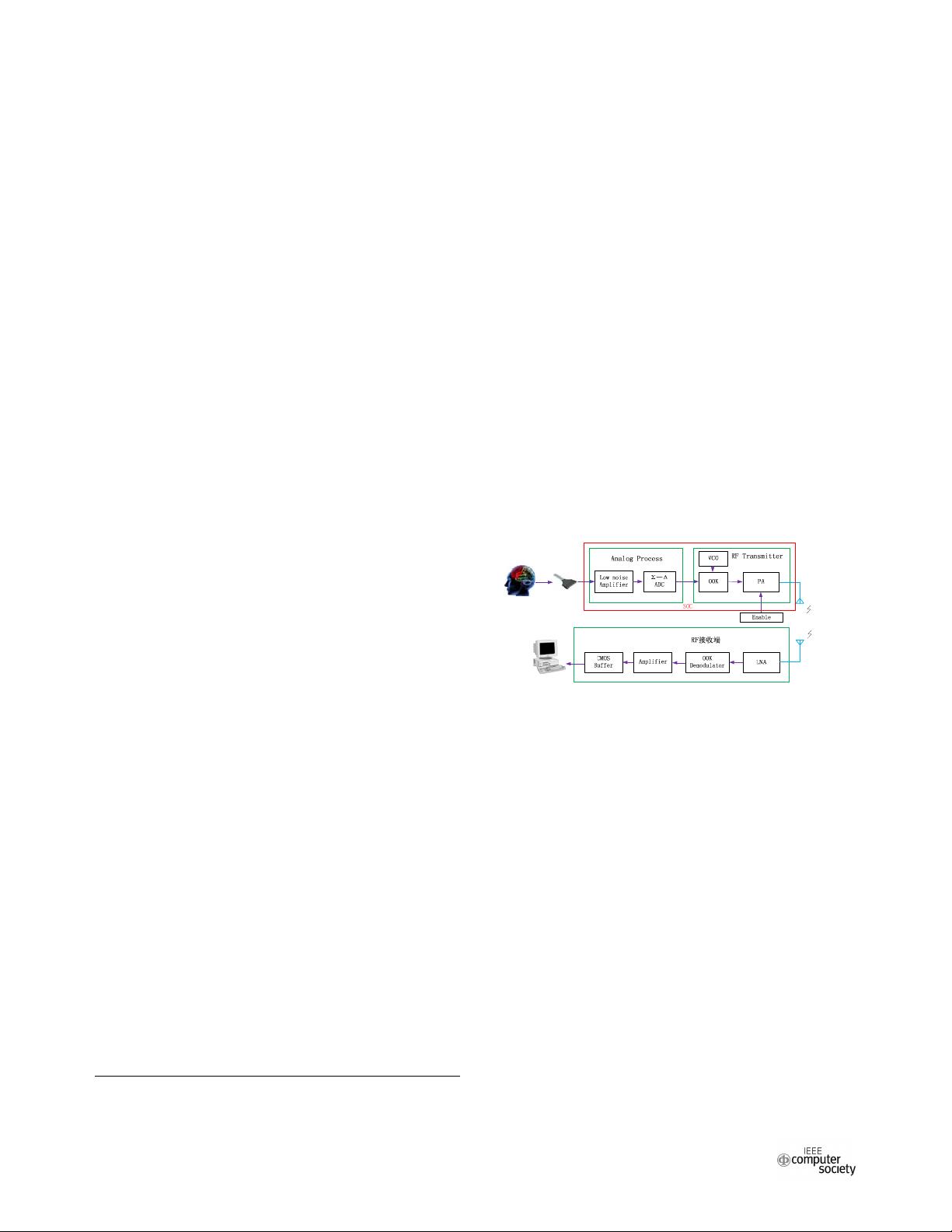
The design proposed in this paper is based on neural signal
acquisition system; the system architecture is shown in Fig. 1.
Analog processing contains low noise amplifier (LNopa) and
ADC. Working frequency of the RF circuits is chosen
according to WIFI and Bluetooth standard (Design frequency is
2.4-2.5GHz), which makes the transmitter a commonly used
interface. OOK modulation is adopted in this design as OOK
has bunch of advantages. The most important one is that this
modulation has nothing to do with the phase information,
which releases the requirement for the carrier signal. Then the
VCO can be used to provide carrier instead of phase locked
loop, which is good for power consumption. Meanwhile, OOK
has the simple circuit implement and less power consumption,
although 1.5 times less bandwidth utilization compared with
Frequency Shift Key modulation method [3]; Carrier signal is
generated by low power VCO. Therefore serial data controls
the OOK modulator on or off, and then the modulated signal
will be sent out by the off-chip antenna after being amplified by
the power amplifier, which transmits data as long as 30 meters.
Fig. 1. Neural acquisition system
B. Analog Processing
Low noise amplifier and ADC are well designed in the
analog processing module: the amplifier is used to acquire
neural signal with a high impedance and low noise
requirements and ADC digitalize the signal for efficient signal
processing.
The following architecture is input stage amplifier that is as
shown in Fig. 2. It is a two stages fully-differential amplifier;
the first stage is common-source amplifier with cross couple
load, the second stage is consisted of a PMOS input
common-source and a NMOS input common-source. The
common mode feedback circuit is a differential input and single
output common source amplifier and capacitors and resistors
are used to collect the common voltage of the main amplifier.
For low noise consideration, input transistors are designed in
large size for lower thermal noise.
This research is supported by the “Strategic Priority Research Program” o
the Chinese Academy of Sciences (Grant No. XDA06020101) and the national
science foundation for young scientists of China (Grant No.61201040).
2013 IEEE International Conference on Green Computing and Communications and IEEE Internet of Things and IEEE Cyber,
Physical and Social Computing
978-0-7695-5046-6/13 $26.00 © 2013 IEEE
DOI 10.1109/GreenCom-iThings-CPSCom.2013.327
1779


