standards, and therefore are capable of interfacing with a greater variety of SDRAM chips. For details,
refer to the device handbook for the target device family.
Synchronizing Clock and Data Signals
The clock for the SDRAM chip (SDRAM clock) must be driven at the same frequency as the clock for the
Avalon-MM interface on the SDRAM controller (controller clock). As in all synchronous designs, you
must ensure that address, data, and control signals at the SDRAM pins are stable when a clock edge
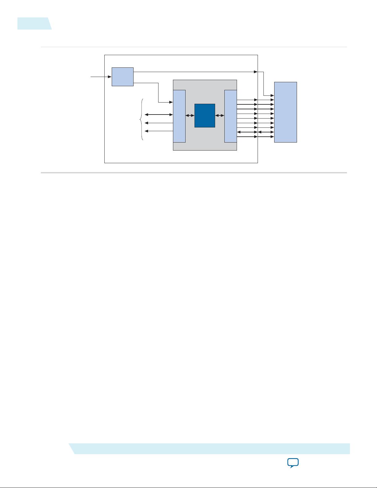
arrives. As shown in the above SDRAM Controller with Avalon Interface block diagram, you can use an
on-chip phase-locked loop (PLL) to alleviate clock skew between the SDRAM controller core and the
SDRAM chip. At lower clock speeds, the PLL might not be necessary. At higher clock rates, a PLL is
necessary to ensure that the SDRAM clock toggles only when signals are stable on the pins. The PLL block
is not part of the SDRAM controller core. If a PLL is necessary, you must instantiate it manually. You can
instantiate the PLL core interface or instantiate an ALTPLL megafunction outside the Qsys system
module.
If you use a PLL, you must tune the PLL to introduce a clock phase shift so that SDRAM clock edges
arrive after synchronous signals have stabilized. See Clock, PLL and Timing Considerations sections for
details.
For more information about instantiating a PLL, refer to PLL Cores chapter. The Nios
®
II development
tools provide example hardware designs that use the SDRAM controller core in conjunction with a PLL,
which you can use as a reference for your custom designs.
The Nios II development tools are available free for download from www.Altera.com.
Clock Enable (CKE) not Supported
The SDRAM controller does not support clock-disable modes. The SDRAM controller permanently
asserts the CKE signal on the SDRAM.
Sharing Pins with other Avalon-MM Tri-State Devices
If an Avalon-MM tri-state bridge is present, the SDRAM controller core can share pins with the existing
tri-state bridge. In this case, the core’s addr, dq (data) and dqm (byte-enable) pins are shared with other
devices connected to the Avalon-MM tri-state bridge. This feature conserves I/O pins, which is valuable in
systems that have multiple external memory chips (for example, flash, SRAM, and SDRAM), but too few
pins to dedicate to the SDRAM chip. See Performance Considerations section for details about how pin
sharing affects performance.
The SDRAM addresses must connect all address bits regardless of the size of the word so that the low-
order address bits on the tri-state bridge align with the low-order address bits on the memory device. The
Avalon-MM tristate address signal always presents a byte address. It is not possible to drop A0 of the tri-
state bridge for memories when the smallest access size is 16 bits or A0-A1 of the tri-state bridge when the
smallest access size is 32 bits.
Board Layout and Pinout Considerations
When making decisions about the board layout and device pinout, try to minimize the skew between the
SDRAM signals. For example, when assigning the device pinout, group the SDRAM signals, including the
SDRAM clock output, physically close together. Also, you can use the Fast Input Register and Fast
Output Register logic options in the Quartus II software. These logic options place registers for the
SDRAM signals in the I/O cells. Signals driven from registers in I/O cells have similar timing characteris‐
tics, such as t
CO
, t
SU
, and t
H
.
UG-01085
2014.24.07
Synchronizing Clock and Data Signals
2-3
SDRAM Controller Core
Altera Corporation
Send Feedback


