Diffractive self-imaging based on selective etching
of a ferroelectric domain inversion grating
Yunlin Chen (陈云琳)*, Tianwei Fan (范天伟), and Man Tong (曼 佟)
Institute of Applied Micro-Nano Materials, School of Science, Beijing Jiaotong University, Beijing 100044, China
*Corresponding author: ylchen@bjtu.edu.cn
Received September 4, 2014; accepted November 28, 2014; posted online February 9, 2015
A hexagonal array grating based on selective etching of a 2D ferroelectric domain inversion in a periodically
poled MgO-doped LiNbO
3
crystal is fabricated. The effects to the diffractive self-imaging as a function of
diffraction distance for a fixed phase difference and array duty cycle of the grating is theoretically analyzed.
The Talbot diffractive self-imaging properties after selective etching of a 2D ferroelectric domain inversion
grating under a fixed phase difference are experimentally demonstrated. A good agreement between theoretical
and experimental results is observed.
OCIS codes: 050.1950, 070.6760, 160.3730.
doi: 10.3788/COL201513.020502.
The phenomenon of self-imaging of periodic objects, also
known as the Talbot effect, was first observed by
Talbot in 1836
[1]
. The field diffracted from a periodic
object illuminated by a plane wave was found to replicate
the object transmittance at certain imaging planes, and
has led to a variety of applications in imaging processing
and synthesis, photolithography, optical testing, optical
metrology, spectrometry, optical computing, as well as
in near-field scanning optical microscopy
[2]
. Particularly,
a Talbot interferometer becomes very useful in X-ray im-
aging due to the lack of efficient lenses for X-rays
[3]
.
The Talbot effect is manifested when a grating is
illuminated with a highly spatially coherent plane wave.
Self-imaging is possible for periodic or also quasi-periodic
objects (i.e., the Montgomery effect
[4]
). The Talbot effect
requires periodic objects, and images are produced solely
by free-space propagation of a diffracted optical field at
integer multiples of Talbot distances. Different optical
elements have been made to exhibit self-imaging based
on the Talbot effect
[5,6]
. Among the various devices, a tun-
able array can be realized with spatial light modulators
(SLMs) based on, for example, liquid crystals. However,
a commercial SLM usually has relatively big pixel dimen-
sions, which limits further applications.
A LiNbO
3
(LN) crystal is a practical material for use in a
Talbot phase array (TPA) due to its perfect optical char-
acteristics
[7]
. However, applying a high externa l electric
field restricts the Talbot diffractive self-imaging (TDSI)
based on periodically poled LN (PPLN) to applications
in optical integration and optical microstructure devices.
PPLN and periodic ally poled LiTaO
3
(PPLT) can be used
to realize second-harmonic self-imaging from 1D PPLN
[8]
,
and second-harmonic Talbot self-imaging from 1D and 2D
PPLT
[9]
. A MgO LN (MgLN) crystal showed a shorter
absorption edge and higher resistance to photorefractive
damage than that of LN
[10]
. Moreover, because of it has a
lower switching field, periodically poled MgLN (PPMgLN)
has been expected to be fairly easily fabricated by means of
electric-field poling
[11]
. These features are important to re-
duce the applied electric field, and improve TPA perfor-
mance. A high flexibility for designing a TPA could be
obtained if arbitrary surface-relief diffractive optical ele-
ments of high quality could be patterned in a MgLN crystal.
Ferroelectric domains of opposite spontaneous polarization
present different etching speeds when dipped in some acid
mixtures. In this work, we theoretically analyzed the effects
on TDSI based on 2D surface-relief diffraction grating from
a diffraction distance. According to the theoretical simula-
tion, we fabricated a 2D surface-relief diffraction grating
based on PPMgLN by selective etching. The TDSI proper-
ties of the selective etching of a 2D ferroelectric domain
inversion grating under a fixed phase difference are exper-
imentally demonstrated.
A 2D hexagonal array grating was designed because of
its high efficiency with respect to luminous energy utiliza-
tion and high compatibility with other optical devices. A
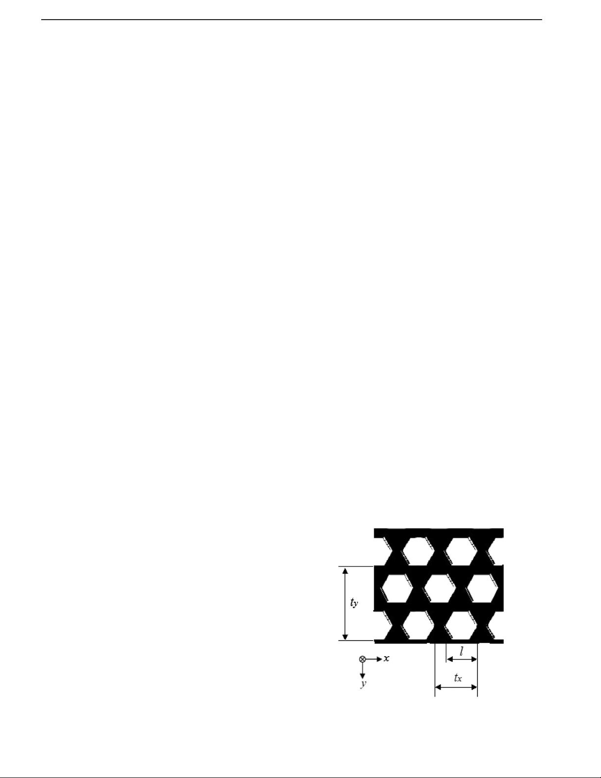
hexagonal ferroelectric domain inversion grating is shown
in Fig. 1, where t
x
and t
y
are the periods in the x and
y-directions (respectively), and the period t
x
¼ 25 μm,
Fig. 1. Hexagonal array grating.
COL 13(2), 020502(2015) CHINESE OPTICS LETTERS February 10, 2015
1671-7694/2015/020502(4) 020502-1 © 2015 Chinese Optics Letters


