www.austriamicrosystems.com Revision 5.5 11 - 53
AS3992
Data Sheet - Detailed Description
7 Detailed Description
The RFID reader IC comprises complete analog and digital functionality for reader operation including transmitter and receiver section with
complete EPC Gen2 or ISO18000-6C digital protocol support. To integrate as many components as possible, the device also comprises an on-
board PLL section with integrated VCO, supply section, DAC and ADC section, and host interface section. In order to cover a wide range of
possibilities, there is also Configuration registers section that configures operation of all blocks.
For operation, the device needs to be correctly supplied via. VEXT and VEXT2 pins and enabled via. EN pin (Refer Supply on page 11 for
connecting to supply and Power Modes on page 12 about operation of the EN pin). At power-up, the configuration registers are preset to a
default operation mode. The preset values are described in the Configuration Registers Address Space on page 23 below each register
description table. It is possible to access and change registers to choose other options.
The communication between the reader and the transponder follows the reader talk first method. After power-up and configuring IC, the host
system starts communication by turning on the RF field by setting option bit rf_on in the ‘Chip status control register’ (00) (see Table 13) and
transmitting the first protocol command (Select in EPC Gen2). Transmitting and receiving is possible in the following two modes:
1. Normal Data Mode: In this mode, the TX and RX data is transferred through the FIFO register and all protocol data processing is done
internally.
2. Direct Data Mode: In this mode, the data processing is done by the host system.
7.1 Supply
The effective supply system of the chip decreases the influence of the supply noise and interference and thus improves de-coupling between
different building blocks. A set of 3.4V regulators is used for supplying the reference block, AD and DA converters, low frequency receiver cells,
the RF part, and digital part. It is possible to use the digital part supply VDD_D for supplying the external MCU with a current consumption up to
20mA. The input pin for the regulators is VEXT. The output pins for regulators are VDD_A, VDD_LF, VDD_D, VDD_RFP and VDD_B. Each of
the pins require stabilizing capacitors to connected ground (2.2…10µF and 10…100nF) in parallel. Depending on quality of the capacitors,
100pF could be required.
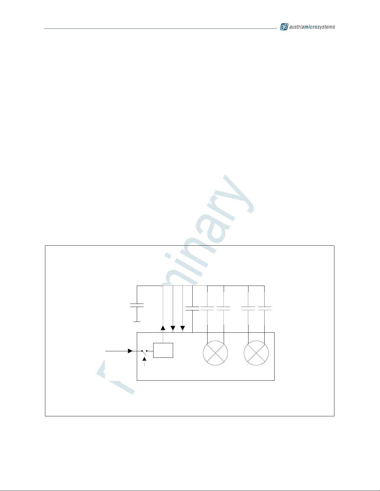
Figure 3. Mixer Supply
An additional 4.8V regulator is used for the input RF mixers supply. The input of this regulator is VEXT, output is VDD_MIX pin. For correct
operation of the 4.8V regulator, the VEXT voltage needs to be between 5.3V and 5.5V. VDD_MIX needs de-coupling capacitors to VDD_MIX like
other VDD pins.
VDD_MIX
VDD_5LFI
VDD_TXPAB
CBV5
COMP_A
COMP_B
COMN_A
COMN_B
Mixer
LDO
VEXT
On
receive


