使用COMSOL进行FEM建模与仿真:ZnO/128°YX LiNbO3层状SAW设备研究
需积分: 50 90 浏览量
更新于2024-09-07
1
收藏 2.03MB PDF 举报
"基于COMSOL的层状SAW设备有限元建模与仿真——ZnO/128°YX LiNbO3结构的研究"
本文深入探讨了使用COMSOL Multiphysics 4.3b平台进行层状表面声波(SAW)设备的建模和仿真技术。COMSOL是一款强大的多物理场仿真软件,它允许用户通过有限元方法(FEM)对复杂的工程问题进行数值模拟,尤其适用于声学、电磁学和热力学等领域。
在该研究中,研究人员关注的是基于ZnO/128°YX LiNbO3材料的SAW设备。SAW设备广泛应用于无线通信和传感器技术,其性能取决于材料的特性以及结构的几何参数。ZnO是一种常见的压电材料,而128°YX LiNbO3则以其优异的声电性能著称。通过改变ZnO层的厚度,研究人员能够研究SAW传播特性如何受到影响。
通过COMSOL的FEM模拟,他们发现SAW设备的频率响应随着ZnO层厚度的变化而变化,范围从166.1MHz降低到150.4MHz。这种变化揭示了SAW传播速度与材料层厚度之间的关键关系,这对于优化设备性能至关重要。
此外,研究还计算了自由相速度(νf)和金属化相速度(νm),这些是评估SAW设备性能的关键参数。利用这些速度,研究人员能够进一步确定结构的机电耦合系数(K2)。K2表示声波能量转化为电信号的能力,是衡量SAW器件效率的重要指标。结果显示,在500nm的ZnO层厚度下,可以获得高达6.05%的耦合系数,这与已发表的数据相符,表明了COMSOL仿真的准确性。
此研究强调了COMSOL在设计和优化SAW设备中的作用,以及通过数值模拟来理解材料参数如何影响声波传播和设备性能的重要性。通过这样的仿真工具,工程师和研究人员可以快速探索设计空间,从而开发出高性能的SAW设备,满足特定应用的需求。对于那些希望深入理解COMSOL在声学和微电子领域应用的人来说,这篇研究提供了一个很好的实例。
FEM Modeling and Simulation of a Layered SAW
device Based on ZnO/128° YX LiNbO
3
Zaid. T. Salim
School of Nano Electronic Engineering
University Malaysia Perlis (UniMAP)
Perlis, Malaysia
zaidtareq86@gmail.com
U. Hashim, and M. K. Md. Arshad
Institution of Nano Electronic Engineering
University Malaysia Perlis (UniMAP)
Perlis, Malaysia
uda@unimap.edu.my
mohd.khairuddin@unimap.edu.my
Abstract—In this paper, the modeling and simulation of a
layered surface acoustic wave device based on ZnO/128° YX
LiNbO
3
were conducted using Finite Element Method (FEM) in
COMSOL Multiphysics 4.3b platform. The SAWs propagation
characteristics were numerically investigated with variation in
the ZnO layer thickness. The results show that the SAW device
frequency response was varied with the ZnO layer thickness
from 166.1 MHz to 150.4 MHz. The free and metalized phase
velocities (
f
and
m
) were calculated and used to calculate the
electromechanical coupling coefficient (K
2
) of the structure. The
results show that a large coupling coefficient of 6.05% can be
obtained in 500 nm ZnO layer thickness which is in a good
agreement with the data published by Nakamura and
Hanamoka.
Keywords—FEM; SAW device; Surface acoustic wave; 128°
YX LiNbO
3
; ZnO
I. INTRODUCTION
Surface acoustic wave devices are used in many types of
electronic components such as filters, resonators and actuators
[1]. Recently, it were investigated both theoretically and
experimentally as gas sensor, pressure sensors, bio sensors and
many other applications such as humidity, magnetic field and
ultrasonic sensors [2-4].A large number of studies were
conducted to develop layered SAW devices by utilizing a
piezoelectric thin film over the substrate to modify the SAW
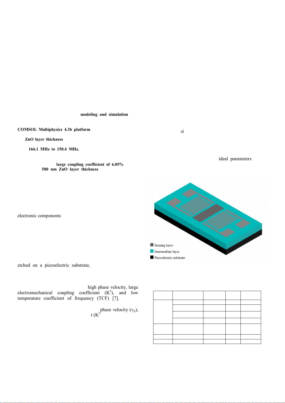
device performance [5]. A typical two-port layered SAW
device is consist of two interdigitated transducers (IDTs)
etched on a piezoelectric substrate, intermediate layer and
sensing layer [6] as illustrated in Fig. 1.
Various factors must be considered in the selection of the
piezoelectric materials used in the SAW device. The
piezoelectric materials must have a high phase velocity, large
electromechanical coupling coefficient (K
2
), and low
temperature coefficient of frequency (TCF) [7]. Table I
summarize the properties of the most common piezoelectric
materials. Choi et al [8] reported that the phase velocity (
p
),
electromechanical coupling coefficient (K
2
) and the sensitivity
can be modified by utilizing a dielectric intermediate layer to
the SAW device structure. Furthermore, Armstrong et al. [9]
reported that when using a piezoelectric thin film over a
piezoelectric substrate, more efficient SAWs can be obtained.
ZnO is a commonly used piezoelectric material due to its
electrical, structural and optical properties. ZnO thin films
were used to generate SAWs over a non-piezoelectric
substrate such as silicon glass and diamond [10-12]. Kalantar-
Zadeh et al. [13] reported that using a ZnO thin film can
increase the SAW device sensitivity compared to SiO
2
in
study using ST-quarts substrate. We can conclude that a pre-
fabrication simulation can help us to investigate the SAW
device performance and select the ideal parameters for the
required application by gaining a better understanding about
the propagation characteristics of the structure.
Fig. 1. Schematic of a typical two-port layered SAW device.
TABLE I. THE MOST COMMON PIEZOELECTRIC MATERIALS USED IN SAW
DEVICES.
Material Orientation/cut
(m/s)
K
2
(%)
TCD
(ppm)/ºC
LiNbO
3
Y-Z 3488 4.5 94
41º Y-X 4751 11.3 50
64º Y-X 4478 17.2 70
128º Y-X 3996 5.5 75
LiTaO
3
77.1º Y-Z
112º X-Y
3254
3300
0.72
0.70
35
18
ZnO
(11-20) 2700 1.1 59-42
SiO
2
47.5º Y-X(ST) 3158 0.11 0
IEEE-ICSE2016 Proc. 2016, Kuala Lumpur, Malaysia
978-1-5090-2383-7/16/$31.00 ©2016 IEEE
5
层状SAW
设备,
基片
振荡
器和
执行
器
利用
符合
层的
功能
来优
化设
备的
功能
好的基
片材料
必须要
包含三
个特
点:1:
高的相
位速
度,2:
大的机
电耦合
系数,
3:低的
频率温
度系数
在一般的基片无法满足一
个滤波器需要的三个要求
时,我们可以使用一个中
间的介电层来改变一个基
片的系数三种基本的系数
由于它的电气,结构和光学特性
基片结构的传播
高
大
低
下载后可阅读完整内容,剩余3页未读,立即下载
2655 浏览量
2118 浏览量
基于Comsol建模与仿真技术的IGBT焊接与压接型单芯片、模块导通及多物理场仿真研究,基于Comsol建模与仿真:IGBT模块的电热力多物理场导通仿真及累积循环次数与截止电场分析,comsol建模与
2025-02-18 上传
基于Comsol建模与仿真:IGBT单芯片及模块的电热力多物理场仿真与累积循环次数分析,comsol建模与仿真 焊接性IGBT、压接型IGBT单芯片、压接型IGBT模块导通的电热力多物理场仿真 累积循
2025-01-30 上传
2025-02-01 上传
罗氏线圈电磁模拟仿真:Comsol建模技术与应用,罗氏线圈的Comsol建模与电磁模拟仿真分析,罗氏线圈comsol建模,电磁模拟仿真 ,罗氏线圈; comsol建模; 电磁模拟仿真,罗氏线圈电磁模拟
2025-03-06 上传
2025-01-29 上传

qq_41862519
- 粉丝: 1
 我的内容管理
展开
我的内容管理
展开


最新资源
- 易二维码签到系统:会议活动签到解决方案
- Ceres库与SDK集成指南:C++环境配置及测试程序
- 深入理解Servlet与JSP技术应用与源码分析
- 初学者指南:掌握VC摄像头抓图源代码实现
- Java实现头像剪裁与上传的camera.swf组件
- FileTime 2013汉化版:单文件修改文件时间的利器
- 波斯语话语项目:实现discourse-persian配置指南
- MP4视频文件数据恢复工具介绍
- 微信与支付宝支付功能封装工具类介绍
- 深入浅出HOOK编程技术与应用
- Jettison 1.0.1源码与Jar包免费下载
- JavaCSV.jar: 解析CSV文档的Java必备工具
- Django音乐网站项目开发指南
- 功能全面的FTP客户端软件FlashFXP_3.6.0.1240_SC发布
- 利用卷积神经网络在Torch 7中实现声学事件检测研究
- 精选网站设计公司官网模板推荐
