REV. D
Information furnished by Analog Devices is believed to be accurate and
reliable. However, no responsibility is assumed by Analog Devices for its
use, nor for any infringements of patents or other rights of third parties
which may result from its use. No license is granted by implication or
otherwise under any patent or patent rights of Analog Devices.
a
Precision, 16 MHz
CBFET Op Amp
AD845
One Technology Way, P.O. Box 9106, Norwood, MA 02062-9106, U.S.A.
Tel: 617/329-4700 Fax: 617/326-8703
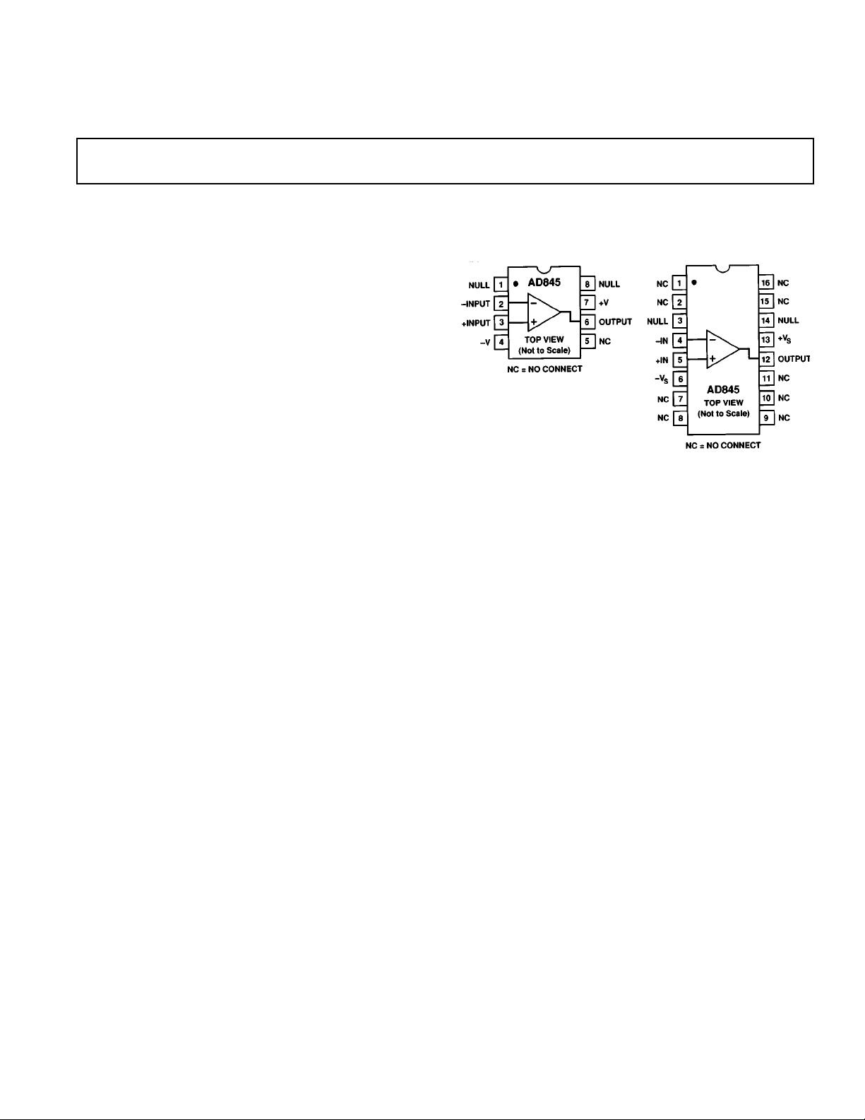
CONNECTION DIAGRAMS
FEATURES
Replaces Hybrid Amplifiers in Many Applications
AC PERFORMANCE:
Settles to 0.01% in 350 ns
100 V/ms Slew Rate
12.8 MHz min Unity-Gain Bandwidth
1.75 MHz Full-Power Bandwidth at 20 V p-p
DC PERFORMANCE:
0.25 mV max Input Offset Voltage
5 mV/8C max Offset Voltage Drift
0.5 nA Input Bias Current
250 V/mV min Open-Loop Gain
4 mV p-p max Voltage Noise, 0.1 Hz to 10 Hz
94 dB min CMRR
Available in Plastic Mini-DIP, Hermetic Cerdip and
SOIC Packages. Also Available in Tape and Reel in
Accordance with EIA-481A Standard
PRODUCT DESCRIPTION
The AD845 is a fast, precise, N channel JFET input, monolithic
operational amplifier. It is fabricated using Analog Devices’
complementary bipolar (CB) process. Advanced laser-wafer
trimming technology enables the very low input offset voltage
and offset voltage drift performance to be realized. This preci-
sion, when coupled with a slew rate of 100 V/µs, a stable
unity-gain bandwidth of 16 MHz, and a settling time of 350 ns
0.01%—while driving a parallel load of 100 pF and 500 Ω—
represents a combination of features unmatched by any FET
input IC amplifier. The AD845 can easily be used to upgrade
many existing designs which use BiFET or FET input hybrid
amplifiers and, in some cases, those which use bipolar input op
amps.
The AD845 is ideal for use in applications such as active filters,
high speed integrators, photo diode preamps, sample-and-hold
amplifiers, log amplifiers, and in buffering A/D and D/A con-
verters. The 250 µV max input offset voltage makes offset null-
ing unnecessary in many applications. The common-mode
rejection ratio of 110 dB over a ±10 V input voltage range
represents exceptional performance for a JFET input high
speed op amp. This, together with a minimum open-loop
gain of 250 V/mV ensures that 12-bit performance is achieved,
even in unity-gain buffer circuits.
The AD845 conforms to the standard op amp pinout except
that offset nulling is to V+. The AD845J and AD845K grade
devices are available specified to operate over the commercial
0°C to +70°C temperature range. AD845A and AD845B
devices are specified for operation over the –40°C to +85°C
industrial temperature range. The AD845S is specified to oper-
ate over the full military temperature range of –55°C to
+125°C. Both the industrial and military versions are available
in 8-pin cerdip packages. The commercial version is available in
an 8-pin plastic mini-DIP and 16-pin SOIC; “J” and “S” grade
chips are also available.
PRODUCT HIGHLIGHTS
1. The high slew rate, fast settling time, and dc precision of the
AD845 make it ideal for high speed applications requiring
12-bit accuracy.
2. The performance of circuits using the LF400, HA2520/2/5,
HA2620/2/5, 3550, OPA605, and LH0062 can be upgraded
in most cases.
3. The AD845 is unity-gain stable and internally compensated.
4. The AD845 is specified while driving 100 pF/500 Ω loads.
Plastic Mini-DIP (N) Package
and Cerdip (Q) Package
16-Pin SOIC
(R-16) Package


