没有合适的资源?快使用搜索试试~ 我知道了~
首页TI ADC09SJ800: 800-MSPS, 9-Bit JESD204C接口模拟数字转换器
TI ADC09SJ800: 800-MSPS, 9-Bit JESD204C接口模拟数字转换器
需积分: 10 0 下载量 108 浏览量
更新于2024-06-28
4
收藏 4.8MB PDF 举报
"TI-ADC09SJ800.pdf" 是一款由TI(德州仪器)推出的高速、高分辨率模拟到数字转换器(ADC),它具备JESD204C串行数据接口,适用于高性能的信号处理系统。
TI的这款ADC09xJ800系列提供四通道(Quad)、双通道(Dual)和单通道(Single Channel)配置,工作速度高达800兆样本每秒(MSPS),并提供了9位的分辨率。其非交织架构设计有助于简化系统集成,而内置的抖动功能则可以降低高阶谐波,提高信号质量。
在性能规格方面,这款ADC在–1dBFS输入时的信噪比(SNR)达到53.5dBFS,表明其在高信号电平时仍能保持良好的噪声抑制。有效位数(ENOB)为8.51位,表示在同样的测试条件下,其实际等效于8.51位的无噪声转换器。此外,它的失真噪声比(SFDR)为64dBFS,意味着在高动态范围下,它能有效地抑制非线性失真。噪声地板(Noise Floor)在–20dBFS时为–140.5 dBFS/Hz,这确保了在低信号电平下的出色噪声表现。
ADC09SJ800的全尺度输入电压为800mV差分峰值对峰值(PP-DIFF),全功率输入带宽高达6GHz,适合处理高频信号。其采用JESD204C标准的串行数据接口,支持2至8条(四通道或双通道)或1至4条(单通道)SerDes线路,最大波特率可达17.16Gbps。接口还支持64B/66B和8B/10B编码模式,以及JESD204B接收机的兼容性。为了实现确定性的延迟,该器件还支持JESD204C的子类1。
此外,ADC09SJ800具有内部采样时钟生成选项,包括内部锁相环(PLL)和压控振荡器(VCO),工作频率范围为7.2至8.2GHz。SYSREF窗口功能用于同步,四个时钟输出简化了系统时钟分配,可为FPGA、相邻ADC及SerDes收发器提供参考时钟。还有时戳输入和输出功能,适用于脉冲系统的精确时间同步。在800MSPS运行时,四通道模式下的功耗数据并未给出,但可以推断,这款ADC在保证高速度的同时,也考虑到了能效。
TI-ADC09SJ800是针对高带宽、高精度应用的理想选择,如通信基础设施、雷达系统、测试与测量设备等,它通过高效的接口和内部时钟管理,为复杂的数字信号处理系统提供了强大的前端转换能力。
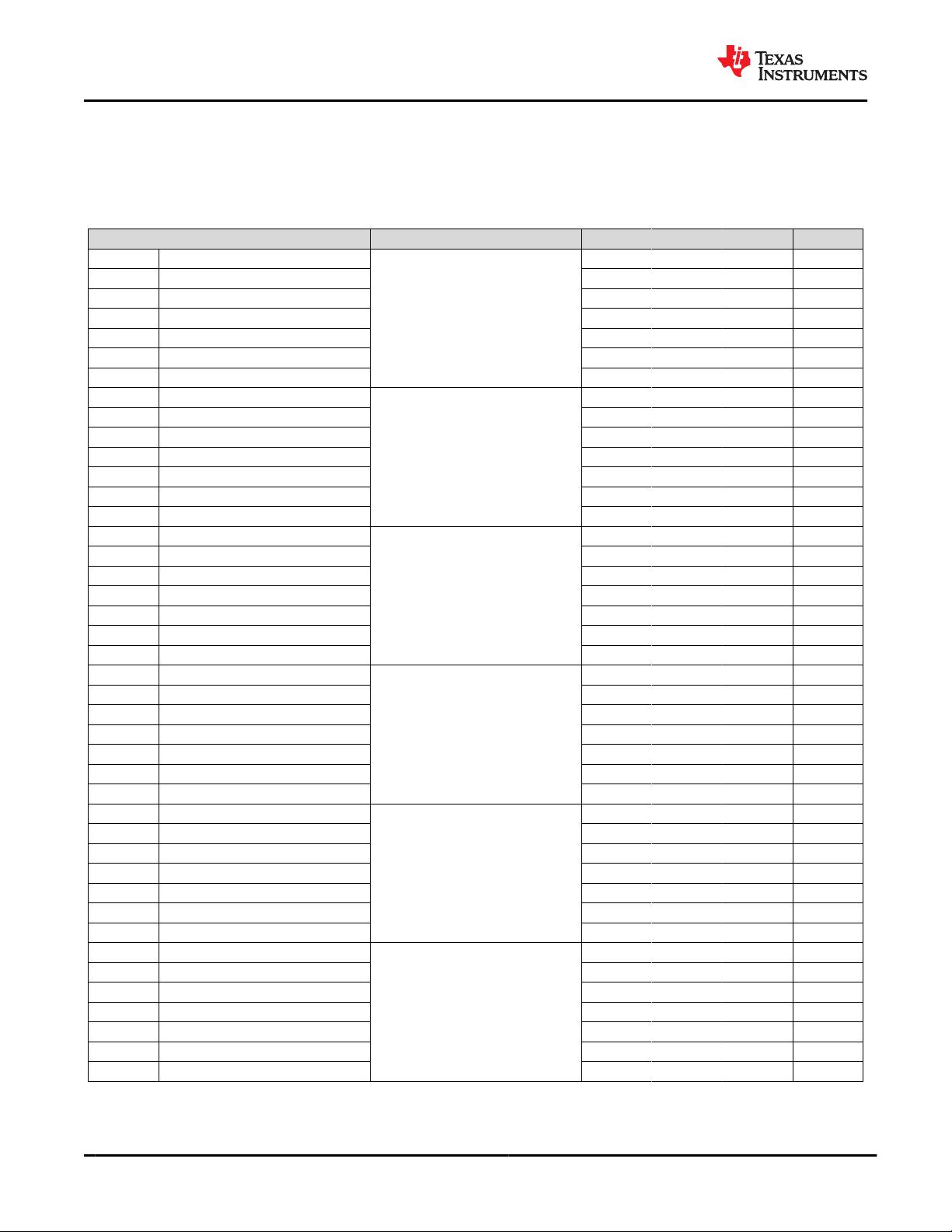
7.6 Electrical Characteristics: Power Consumption
typical values at T
A
= 25°C, VA19 = 1.9 V, VPLL19 = 1.9 V, VREFO = 1.9 V, VTRIG = 1.1V, VA11 = 1.1 V, VD11 = 1.1 V,
default full-scale voltage (V
FS
= 0.8 V
PP
), f
IN
= 97 MHz, A
IN
= –1 dBFS, f
CLK
= 800 MSPS, filtered 1 V
PP
sine-wave clock
applied to CLK±, PLL disabled, JMODE = 0, High Performance Mode and foreground calibration (unless otherwise noted);
minimum and maximum values are at nominal supply voltages and over the operating free-air temperature range provided in
the Recommended Operating Conditions table
PARAMETER TEST CONDITIONS MIN TYP MAX UNIT
I
VA19
1.9-V analog supply current
Power mode 1a: Quad channel, JMODE
0 (9-bit, 8 lanes, 8B/10B encoding), FG
calibration, PLL_EN = 0, f
S
= 800 MSPS,
High Performance Mode
664 mA
I
VPLL19
PLL analog supply current 0 mA
I
VREFO
PLLREFO± analog supply current 0 mA
I
VTRIG
TRIGOUT± analog supply current 0 mA
I
VA11
1.1-V analog supply current 461 mA
I
VD11
1.1-V digital supply current 384 mA
P
DIS
Power dissipation 2.18 W
I
VA19
1.9-V analog supply current
Power mode 1b: Dual channel, JMODE
0 (9-bit, 8 lanes, 8B/10B encoding), FG
calibration, PLL_EN = 0, f
S
= 800 MSPS,
High Performance Mode
388 mA
I
VPLL19
PLL analog supply current 0 mA
I
VREFO
PLLREFO± analog supply current 0 mA
I
VTRIG
TRIGOUT± analog supply current 0 mA
I
VA11
1.1-V analog supply current 346 mA
I
VD11
1.1-V digital supply current 243 mA
P
DIS
Power dissipation 1.38 W
I
VA19
1.9-V analog supply current
Power mode 1c: Single channel, JMODE
0 (9-bit, 8 lanes, 8B/10B encoding), FG
calibration, PLL_EN = 0, f
S
= 800 MSPS,
High Performance Mode
255 mA
I
VPLL19
PLL analog supply current 0 mA
I
VREFO
PLLREFO± analog supply current 0 mA
I
VTRIG
TRIGOUT± analog supply current 0 mA
I
VA11
1.1-V analog supply current 321 mA
I
VD11
1.1-V digital supply current 160 mA
P
DIS
Power dissipation 1.01 W
I
VA19
1.9-V analog supply current
Power mode 2a: Quad channel, JMODE 8
(9-bit, 4 lanes, 64B/66B encoding), LPBG
calibration, PLL_EN = 0, f
S
= 800 MSPS,
Low Power Mode
574 mA
I
VPLL19
PLL analog supply current 0 mA
I
VREFO
PLLREFO± analog supply current 0 mA
I
VTRIG
TRIGOUT± analog supply current 0 mA
I
VA11
1.1-V analog supply current 355 mA
I
VD11
1.1-V digital supply current 326 mA
P
DIS
Power dissipation 1.84
(1)
W
I
VA19
1.9-V analog supply current
Power mode 2b: Dual channel, JMODE 8
(9-bit, 4 lanes, 64B/66B encoding), LPBG
calibration, PLL_EN = 0, f
S
= 800 MSPS,
Low Power Mode
346 mA
I
VPLL19
PLL analog supply current 0 mA
I
VREFO
PLLREFO± analog supply current 0 mA
I
VTRIG
TRIGOUT± analog supply current 0 mA
I
VA11
1.1-V analog supply current 306 mA
I
VD11
1.1-V digital supply current 199 mA
P
DIS
Power dissipation 1.21
(1)
W
I
VA19
1.9-V analog supply current
Power mode 2c: Single channel, JMODE
8 (9-bit, 4 lanes, 64B/66B encoding),
LPBG calibration, PLL_EN = 0, f
S
= 800
MSPS, Low Power Mode
237 mA
I
VPLL19
PLL analog supply current 0 mA
I
VREFO
PLLREFO± analog supply current 0 mA
I
VTRIG
TRIGOUT± analog supply current 0 mA
I
VA11
1.1-V analog supply current 282 mA
I
VD11
1.1-V digital supply current 147 mA
P
DIS
Power dissipation 0.92
(1)
W
ADC09QJ800, ADC09DJ800, ADC09SJ800
SBASAG1 – OCTOBER 2021
www.ti.com
16 Submit Document Feedback
Copyright © 2021 Texas Instruments Incorporated
Product Folder Links: ADC09QJ800 ADC09DJ800 ADC09SJ800
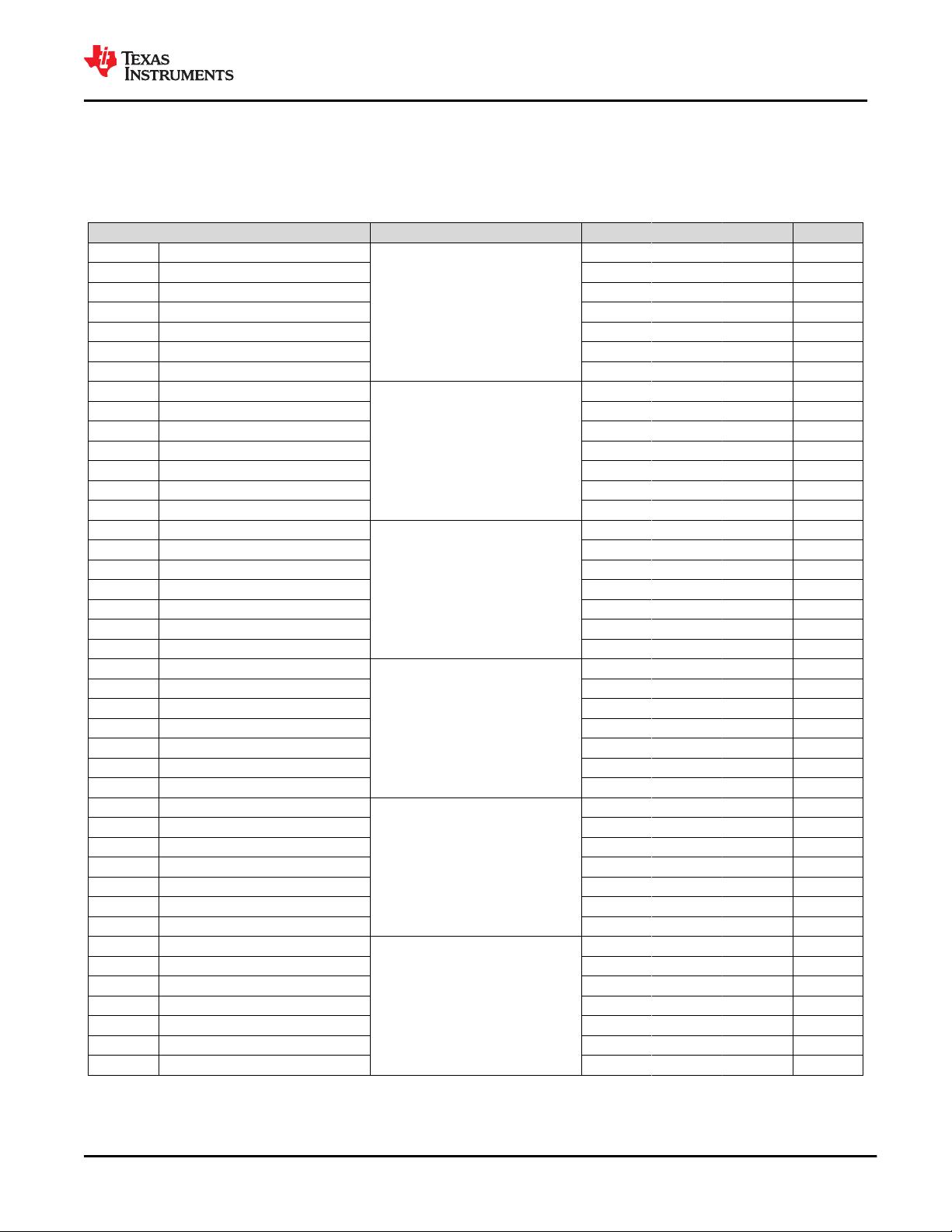
7.6 Electrical Characteristics: Power Consumption (continued)
typical values at T
A
= 25°C, VA19 = 1.9 V, VPLL19 = 1.9 V, VREFO = 1.9 V, VTRIG = 1.1V, VA11 = 1.1 V, VD11 = 1.1 V,
default full-scale voltage (V
FS
= 0.8 V
PP
), f
IN
= 97 MHz, A
IN
= –1 dBFS, f
CLK
= 800 MSPS, filtered 1 V
PP
sine-wave clock
applied to CLK±, PLL disabled, JMODE = 0, High Performance Mode and foreground calibration (unless otherwise noted);
minimum and maximum values are at nominal supply voltages and over the operating free-air temperature range provided in
the Recommended Operating Conditions table
PARAMETER TEST CONDITIONS MIN TYP MAX UNIT
I
VA19
1.9-V analog supply current
Power mode 3a: Quad channel, JMODE 8
(9-bit, 4 lanes, 64B/66B encoding), LPBG
calibration, PLL_EN = 1, PLLREF_SE = 1,
f
REF
= 50 MHz, TRIGOUT± enabled, f
S
=
800 MSPS, Low Power Mode
575 mA
I
VPLL19
PLL analog supply current 60 mA
I
VREFO
PLLREFO± analog supply current 13 mA
I
VTRIG
TRIGOUT± analog supply current 5.5 mA
I
VA11
1.1-V analog supply current 340 mA
I
VD11
1.1-V digital supply current 325 mA
P
DIS
Power dissipation 1.97
(1)
W
I
VA19
1.9-V analog supply current
Power mode 3b: Dual channel, JMODE 8
(9-bit, 4 lanes, 64B/66B encoding), LPBG
calibration, PLL_EN = 1, PLLREF_SE = 1,
f
REF
= 50 MHz, TRIGOUT± enabled, f
S
=
800 MSPS, Low Power Mode
348 mA
I
VPLL19
PLL analog supply current 59 mA
I
VREFO
PLLREFO± analog supply current 13 mA
I
VTRIG
TRIGOUT± analog supply current 5.5 mA
I
VA11
1.1-V analog supply current 290 mA
I
VD11
1.1-V digital supply current 198 mA
P
DIS
Power dissipation 1.34
(1)
W
I
VA19
1.9-V analog supply current
Power mode 3c: Single channel,
JMODE 8 (9-bit, 4 lanes, 64B/66B
encoding), LPBG calibration, PLL_EN =
1, PLLREF_SE = 1, f
REF
= 50 MHz,
TRIGOUT± enabled, f
S
= 800 MSPS, Low
Power Mode
238 mA
I
VPLL19
PLL analog supply current 59 mA
I
VREFO
PLLREFO± analog supply current 13 mA
I
VTRIG
TRIGOUT± analog supply current 5.5 mA
I
VA11
1.1-V analog supply current 265 mA
I
VD11
1.1-V digital supply current 148 mA
P
DIS
Power dissipation 1.06
(1)
W
I
VA19
1.9-V analog supply current
Power mode 4a: Quad channel, JMODE
7 (8-bit, 4 lanes, 64B/66B encoding), FG
calibration, PLL_EN = 0, f
S
= 800 MSPS,
Low Power Mode
550 mA
I
VPLL19
PLL analog supply current 0 mA
I
VREFO
PLLREFO± analog supply current 0 mA
I
VTRIG
TRIGOUT± analog supply current 0 mA
I
VA11
1.1-V analog supply current 330 mA
I
VD11
1.1-V digital supply current 245 mA
P
DIS
Power dissipation 1.68 W
I
VA19
1.9-V analog supply current
Power mode 4b: Dual channel, JMODE
7 (8-bit, 4 lanes, 64B/66B encoding), FG
calibration, PLL_EN = 0, f
S
= 800-MSPS,
Low Power Mode
333 mA
I
VPLL19
PLL analog supply current 0 mA
I
VREFO
PLLREFO± analog supply current 0 mA
I
VTRIG
TRIGOUT± analog supply current 0 mA
I
VA11
1.1-V analog supply current 283 mA
I
VD11
1.1-V digital supply current 152 mA
P
DIS
Power dissipation 1.11 W
I
VA19
1.9-V analog supply current
Power mode 4c: Single channel, JMODE
7 (8-bit, 4 lanes, 64B/66B encoding), FG
calibration, PLL_EN = 0, f
S
= 800-MSPS,
Low Power Mode
224 mA
I
VPLL19
PLL analog supply current 0 mA
I
VREFO
PLLREFO± analog supply current 0 mA
I
VTRIG
TRIGOUT± analog supply current 0 mA
I
VA11
1.1-V analog supply current 260 mA
I
VD11
1.1-V digital supply current 112 mA
P
DIS
Power dissipation 0.84 W
www.ti.com
ADC09QJ800, ADC09DJ800, ADC09SJ800
SBASAG1 – OCTOBER 2021
Copyright © 2021 Texas Instruments Incorporated
Submit Document Feedback
17
Product Folder Links: ADC09QJ800 ADC09DJ800 ADC09SJ800
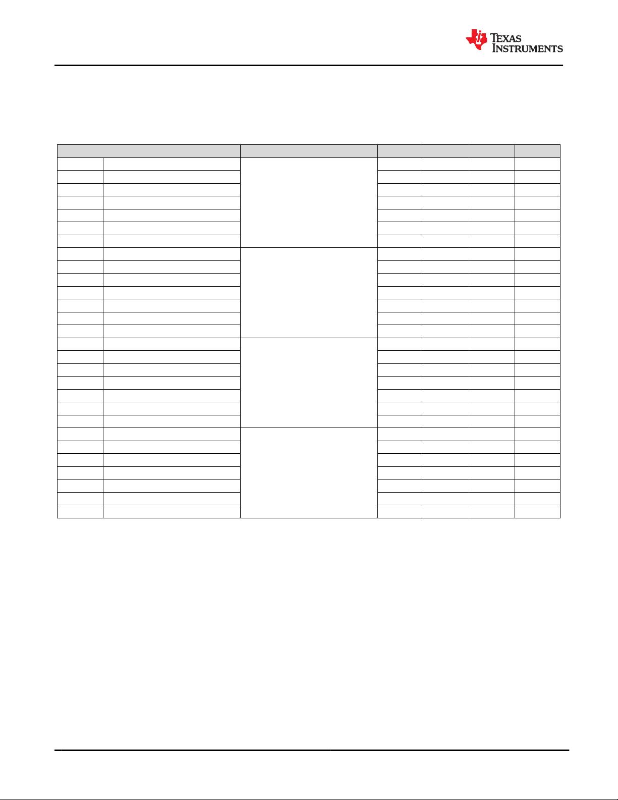
7.6 Electrical Characteristics: Power Consumption (continued)
typical values at T
A
= 25°C, VA19 = 1.9 V, VPLL19 = 1.9 V, VREFO = 1.9 V, VTRIG = 1.1V, VA11 = 1.1 V, VD11 = 1.1 V,
default full-scale voltage (V
FS
= 0.8 V
PP
), f
IN
= 97 MHz, A
IN
= –1 dBFS, f
CLK
= 800 MSPS, filtered 1 V
PP
sine-wave clock
applied to CLK±, PLL disabled, JMODE = 0, High Performance Mode and foreground calibration (unless otherwise noted);
minimum and maximum values are at nominal supply voltages and over the operating free-air temperature range provided in
the Recommended Operating Conditions table
PARAMETER TEST CONDITIONS MIN TYP MAX UNIT
I
VA19
1.9-V analog supply current
Power mode 5a: Quad channel, JMODE
0 (9-bit, 8 lanes, 8B/10B encoding), BG
calibration, PLL_EN = 1, PLLREF_SE = 0,
f
REF
= 50 MHz, TRIGOUT± enabled, f
S
=
800 MSPS, High Performance Mode
814 mA
I
VPLL19
PLL analog supply current 60 mA
I
VREFO
PLLREFO± analog supply current 13 mA
I
VTRIG
TRIGOUT± analog supply current 5.5 mA
I
VA11
1.1-V analog supply current 522 mA
I
VD11
1.1-V digital supply current 384 mA
P
DIS
Power dissipation 2.68 W
I
VA19
1.9-V analog supply current
Power mode 5b: Dual channel, JMODE
0 (9-bit, 8 lanes, 8B/10B encoding), BG
calibration, PLL_EN = 1, PLLREF_SE = 0,
f
REF
= 50 MHz, TRIGOUT± enabled, f
S
=
800 MSPS, High Performance Mode
524 mA
I
VPLL19
PLL analog supply current 58 mA
I
VREFO
PLLREFO± analog supply current 13 mA
I
VTRIG
TRIGOUT± analog supply current 5.5 mA
I
VA11
1.1-V analog supply current 398 mA
I
VD11
1.1-V digital supply current 247 mA
P
DIS
Power dissipation 1.85 W
I
VA19
1.9-V analog supply current
Power mode 5c: Single channel, JMODE
0 (9-bit, 8 lanes, 8B/10B encoding), BG
calibration, PLL_EN = 1, PLLREF_SE = 0,
f
REF
= 50 MHz, TRIGOUT± enabled, f
S
=
800 MSPS, High Performance Mode
386 mA
I
VPLL19
PLL analog supply current 58 mA
I
VREFO
PLLREFO± analog supply current 13 mA
I
VTRIG
TRIGOUT± analog supply current 5.5 mA
I
VA11
1.1-V analog supply current 368 mA
I
VD11
1.1-V digital supply current 158 mA
P
DIS
Power dissipation 1.46 W
I
VA19
1.9-V analog supply current
Power mode 6: Power-down enabled (PD
= 1)
47 mA
I
VPLL19
PLL analog supply current 0 mA
I
VREFO
PLLREFO± analog supply current 0 mA
I
VTRIG
TRIGOUT± analog supply current 0 mA
I
VA11
1.1-V analog supply current 32 mA
I
VD11
1.1-V digital supply current 23.7 mA
P
DIS
Power dissipation 0.15 W
(1) Low-power background (LPBG) calibration supply current and power dissipation numbers are in the calibration sleep state. The power
dissipation in this mode increases to the background (BG) calibration power consumption during the calibration state. The sleep period
can be controlled by the user and long sleep periods will average out the calibration state power dissipation contribution.
ADC09QJ800, ADC09DJ800, ADC09SJ800
SBASAG1 – OCTOBER 2021
www.ti.com
18 Submit Document Feedback
Copyright © 2021 Texas Instruments Incorporated
Product Folder Links: ADC09QJ800 ADC09DJ800 ADC09SJ800
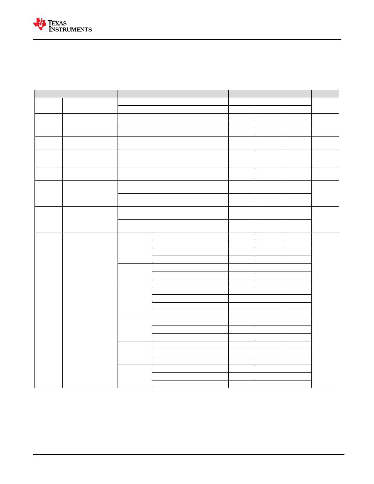
7.7 Electrical Characteristics: AC Specifications
typical values at T
A
= 25°C, VA19 = 1.9 V, VPLL19 = 1.9 V, VREFO = 1.9 V, VTRIG = 1.1V, VA11 = 1.1 V, VD11 = 1.1
V, default full-scale voltage (V
FS
= 0.8 V
PP
), f
IN
= 97 MHz, A
IN
= –1 dBFS, f
CLK
= 800 MHz, filtered 1 V
PP
sine-wave clock
applied to CLK±, PLL disabled, JMODE = 0, High Performance Mode and foreground calibration (unless otherwise noted);
minimum and maximum values are at nominal supply voltages and over the operating free-air temperature range provided in
the Recommended Operating Conditions table
PARAMETER TEST CONDITIONS MIN TYP MAX UNIT
FPBW
Full-power input bandwidth
(–3 dB)
(1)
Foreground calibration 6
GHz
Background calibration 6
XTALK
Channel-to-channel
crosstalk
(Quad and dual channel
only)
Aggressor = 400 MHz, –1 dBFS –80
dBAggressor = 1 GHz, –1 dBFS –65
Aggressor = 3 GHz, –1 dBFS –62
CER Code error rate
Maximum CER, does not include JESD204C interface
BER
10
–18
Errors/
sample
t
ORR
Overrange recovery time
Time from an overdriven input to accurate conversion
after a step from a ±1.2 V
PP-DIFF
overdriven input
stepped to 0 V
PP-DIFF
.
1 t
CLK
cycles
NOISE
DC
DC input noise standard
deviation
No input, foreground calibration, excludes DC offset 0.27 LSB
NSD Noise spectral density
Maximum full-scale voltage (V
FS
= 1.0 V
PP
), A
IN
= –20
dBFS
–140.5
dBFS/Hz
Default full-scale voltage (V
FS
= 0.8 V
PP
), A
IN
= –20
dBFS
–140
NF Noise figure, Z
S
= 100 Ω
Maximum full-scale voltage (V
FS
= 1.0 V
PP
), A
IN
= –20
dBFS
34.4
dB
Default full-scale voltage (V
FS
= 0.8 V
PP
), A
IN
= –20
dBFS
33
SNR
Signal-to-noise ratio,
excluding DC, HD2 to HD9
f
IN
= 97 MHz
A
IN
= –1 dBFS 53.5
dBFS
A
IN
= –3 dBFS 53.7
A
IN
= –12 dBFS 54
A
IN
= –3 dBFS, V
FS
= 1.0 V
PP
54
f
IN
= 497 MHz
A
IN
= –1 dBFS 53.7
A
IN
= –3 dBFS 53.7
A
IN
= –12 dBFS 53.9
f
IN
= 997 MHz
A
IN
= –1 dBFS 51 53.5
A
IN
= –3 dBFS 53.5
A
IN
= –12 dBFS 53.9
A
IN
= –3 dBFS, V
FS
= 1.0 V
PP
53.8
f
IN
= 1797 MHz
A
IN
= –1 dBFS 53.2
A
IN
= –3 dBFS 53.5
A
IN
= –12 dBFS 53.8
f
IN
= 2697 MHz
A
IN
= –1 dBFS 52.5
A
IN
= –3 dBFS 52.6
A
IN
= –12 dBFS 53.8
f
IN
= 3497 MHz
A
IN
= –1 dBFS 52.6
A
IN
= –3 dBFS 53.1
A
IN
= –12 dBFS 53.8
www.ti.com
ADC09QJ800, ADC09DJ800, ADC09SJ800
SBASAG1 – OCTOBER 2021
Copyright © 2021 Texas Instruments Incorporated
Submit Document Feedback
19
Product Folder Links: ADC09QJ800 ADC09DJ800 ADC09SJ800
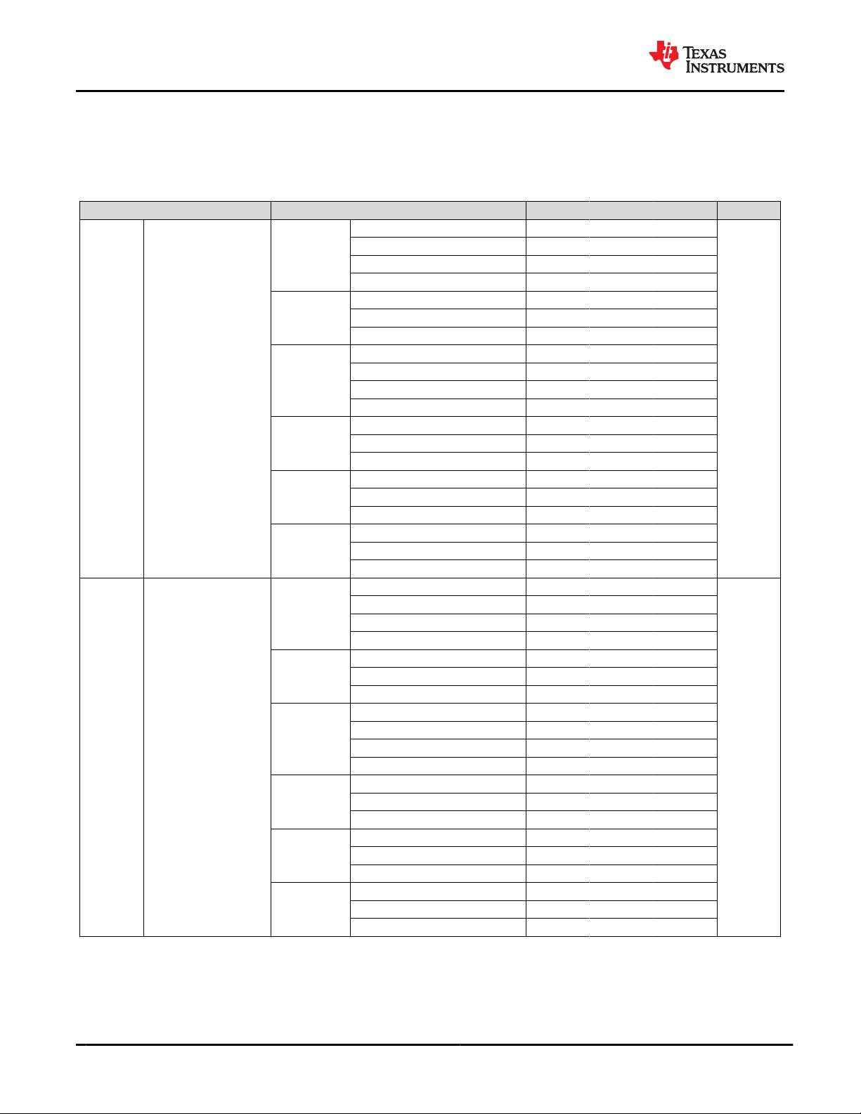
7.7 Electrical Characteristics: AC Specifications (continued)
typical values at T
A
= 25°C, VA19 = 1.9 V, VPLL19 = 1.9 V, VREFO = 1.9 V, VTRIG = 1.1V, VA11 = 1.1 V, VD11 = 1.1
V, default full-scale voltage (V
FS
= 0.8 V
PP
), f
IN
= 97 MHz, A
IN
= –1 dBFS, f
CLK
= 800 MHz, filtered 1 V
PP
sine-wave clock
applied to CLK±, PLL disabled, JMODE = 0, High Performance Mode and foreground calibration (unless otherwise noted);
minimum and maximum values are at nominal supply voltages and over the operating free-air temperature range provided in
the Recommended Operating Conditions table
PARAMETER TEST CONDITIONS MIN TYP MAX UNIT
SINAD
Signal-to-noise and
distortion ratio, excluding
DC offset
f
IN
= 97 MHz
A
IN
= –1 dBFS 53
dBFS
A
IN
= –3 dBFS 52.7
A
IN
= –12 dBFS 53.8
A
IN
= –3 dBFS, V
FS
= 1.0 V
PP
53.4
f
IN
= 497 MHz
A
IN
= –1 dBFS 53.4
A
IN
= –3 dBFS 53.6
A
IN
= –12 dBFS 53.8
f
IN
= 997 MHz
A
IN
= –1 dBFS 51 53.1
A
IN
= –3 dBFS 53.4
A
IN
= –12 dBFS 53.8
A
IN
= –3 dBFS, V
FS
= 1.0 V
PP
53.6
f
IN
= 1797 MHz
A
IN
= –1 dBFS 52.6
A
IN
= –3 dBFS 53.3
A
IN
= –12 dBFS 53.8
f
IN
= 2697 MHz
A
IN
= –1 dBFS 49.7
A
IN
= –3 dBFS 51.8
A
IN
= –12 dBFS 53.8
f
IN
= 3497 MHz
A
IN
= –1 dBFS 46.7
A
IN
= –3 dBFS 51.2
A
IN
= –12 dBFS 53.7
ENOB
Effective number of bits,
excluding DC offset
f
IN
= 97 MHz
A
IN
= –1 dBFS 8.51
bits
A
IN
= –3 dBFS 8.46
A
IN
= –12 dBFS 8.6
A
IN
= –3 dBFS, V
FS
= 1.0 V
PP
8.58
f
IN
= 497 MHz
A
IN
= –1 dBFS 8.57
A
IN
= –3 dBFS 8.61
A
IN
= -12 dBFS 8.64
f
IN
= 997 MHz
A
IN
= –1 dBFS 8.1 8.55
A
IN
= –3 dBFS 8.6
A
IN
= –12 dBFS 8.7
A
IN
= –3 dBFS, V
FS
= 1.0 V
PP
8.6
f
IN
= 1797 MHz
A
IN
= –1 dBFS 8.44
A
IN
= –3 dBFS 8.56
A
IN
= –12 dBFS 8.63
f
IN
= 2697 MHz
A
IN
= –1 dBFS 7.9
A
IN
= –3 dBFS 8.3
A
IN
= –12 dBFS 8.6
f
IN
= 3497 MHz
A
IN
= –1 dBFS 7.63
A
IN
= –3 dBFS 8.21
A
IN
= –12 dBFS 8.62
ADC09QJ800, ADC09DJ800, ADC09SJ800
SBASAG1 – OCTOBER 2021
www.ti.com
20 Submit Document Feedback
Copyright © 2021 Texas Instruments Incorporated
Product Folder Links: ADC09QJ800 ADC09DJ800 ADC09SJ800
剩余150页未读,继续阅读
不觉明了
- 粉丝: 6308
- 资源: 5764
上传资源 快速赚钱
 我的内容管理
展开
 我的资源
快来上传第一个资源
 我的收益 登录查看自己的收益
 我的积分
登录查看自己的积分
 我的C币
登录后查看C币余额
 我的收藏
我的收藏  我的下载
我的下载  下载帮助
下载帮助

最新资源
- d3-Scatterplot-Graph-fcc:FreeCodeCamp d3散点图
- CG引擎:一个随机的家伙,很开心创建c ++ OpenGl游戏引擎
- Linux shell脚本.rar
- UltrasonicDistanceMeasurementSystem:超声波测距,报警,LCD1602显示数据,温度校正超声波速度
- Excel模板基础体温记录表excel版.zip
- Advanced-Factorization-of-Machine-Systems:GSOC 2017-Apache组织-#使用并行随机梯度下降(python和scala)在Spark上实现分解机器
- operating_system_concept_os
- dosxnt文件-DOS其他资源
- Smart-Device:对于htmlacademy
- static-form-lambda:无服务器模板,创建一个FaaS AWS Lambda来处理表单提交
- Python库 | python-jose-0.6.1.tar.gz
- :scissors: React-Native 组件可在您想要的任何地方切割触摸Kong。 教程叠加的完美解决方案
- ocr
- react-pwa:使用creat js的示例渐进式Web应用程序
- VBiosFinder:从(几乎)任何BIOS更新中提取嵌入式VBIOS
- Python库 | python-hpilo-2.4.tar.gz
安全验证
文档复制为VIP权益,开通VIP直接复制
 信息提交成功