TI-TCA9548A-Q1: 汽车级8通道I2C开关与功能安全设计
需积分: 0 200 浏览量
更新于2024-06-27
4
收藏 1.15MB PDF 举报
TI-TCA9548A-Q1是一款专为汽车应用设计的高性能I2C开关,它符合AEC-Q100等级1标准,确保在严苛的汽车环境中稳定运行。该芯片提供了八路双向转换开关,每个通道均可通过I2C总线独立控制,允许灵活的I2C地址映射,解决多路设备共享同一地址的问题,例如在连接多个相同数字温度传感器时。
其主要特性包括:
1. 功能安全:提供详细的文档支持,帮助设计者构建安全可靠的功能系统。
2. 低电平有效的复位输入:当系统控制器检测到故障时,可通过复位信号轻松重启TCA9548A-Q1,无需中断供电。
3. 多种电压兼容性:支持1.8V、2.5V、3.3V和5V电压等级间的切换,允许不同电压的设备间通信。
4. 热插拔和低静态电流:设计考虑了实时操作的灵活性,同时保持较低的能耗。
5. 宽广的工作电源电压范围:1.65V至5.25V,适应各种供电环境。
6. 低阻抗开关:RON值低,有助于减少信号传输损耗。
7. 高速接口:支持400kHz的时钟频率,满足高速数据传输需求。
8. 闩锁性能:超过100mA的电流处理能力,符合JESD78II类规范,保证信号完整性。
在应用方面,TCA9548A-Q1广泛用于信息娱乐系统、车身控制、电信交换设备(如路由器)、工厂自动化以及存在I2C地址冲突的场景,如多个温度传感器。
使用时,用户可以通过编程寄存器来配置各个通道的开关状态,上电时默认所有通道关闭。器件的VCC引脚用于限制最高电压传输,外部上拉电阻则用于调整各通道的电压水平,使其与不同的设备兼容。所有I/O引脚能承受高达5V的电压,确保信号完整性。
TCA9548A-Q1的封装形式为VQFN(24),尺寸为4.00mm×4.00mm,如需了解更多封装选项,请查阅数据表中的可订购产品附录。这款I2C开关是汽车电子系统中不可或缺的组件,提供了高效、可靠和灵活的I2C扩展解决方案。
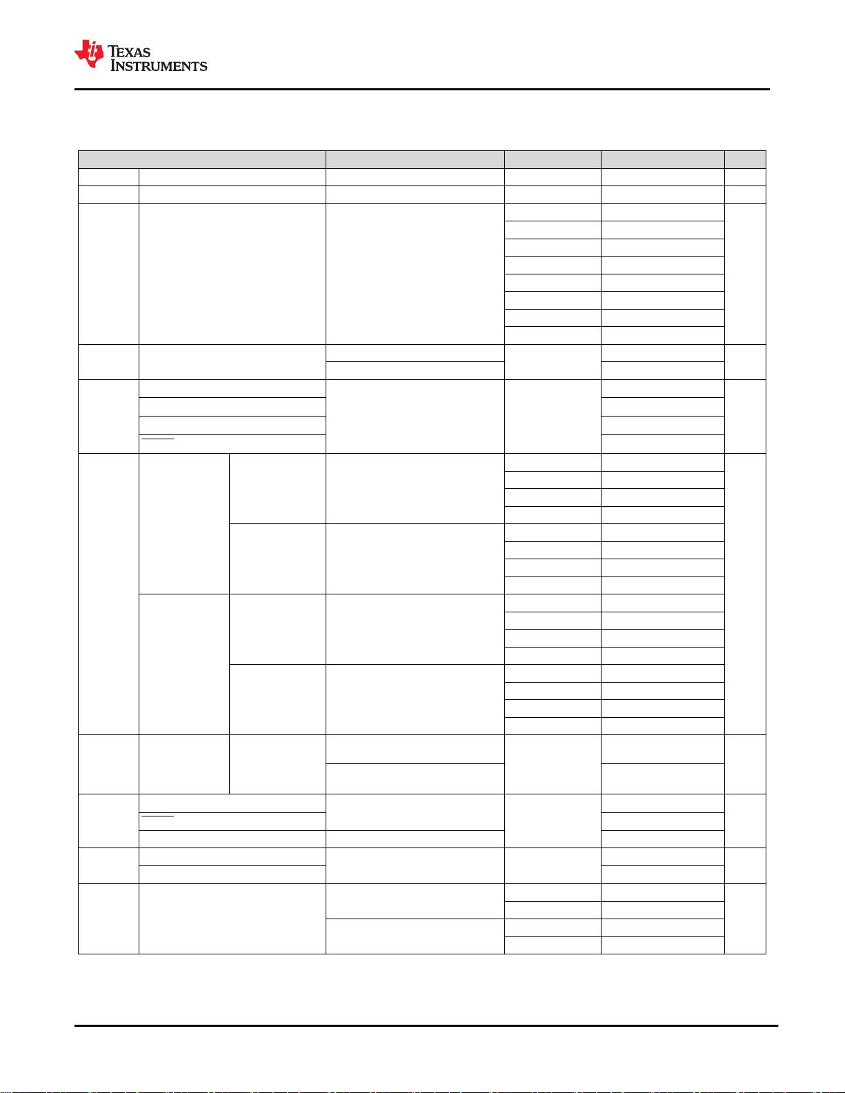
6.5 Electrical Characteristics
(1)
over recommended operating free-air temperature range (unless otherwise noted)
PARAMETER TEST CONDITIONS V
CC
MIN TYP MAX UNIT
V
PORR
Power-on reset voltage, V
CC
rising No load, V
I
= V
CC
or GND
(4)
1.2 1.5 V
V
PORF
Power-on reset voltage, V
CC
falling
(2)
No load, V
I
= V
CC
or GND
(4)
0.8 1 V
V
o(sw)
Switch output voltage
V
i(sw)
= V
CC
, I
SWout
= –100 μA
5 V 3.6
V
4.5 V to 5.25 V 2.6 4.5
3.3 V 1.9
3 V to 3.6 V 1.6 2.8
2.5 V 1.5
2.3 V to 2.7 V 1.1 2
1.8 V 1.1
1.65 V to 1.95 V 0.6 1.25
I
OL
SDA
V
OL
= 0.4 V
1.65 V to 5.25 V
3 6
mA
V
OL
= 0.6 V 5 9
I
I
SCL, SDA
V
I
= V
CC
or GND
(4)
1.65 V to 5.25 V
–1
1
μA
SC7–SC0, SD7–SD0 –1
1
A2–A0 –1
1
RESET
–1
1
I
CC
Operating mode
f
SCL
= 400 kHz V
I
= V
CC
or GND
(4)
, I
O
= 0
5.25 V 50 80
μA
3.6 V 20 35
2.7 V 11 20
1.65 V 6 10
f
SCL
= 100 kHz V
I
= V
CC
or GND
(4)
, I
O
= 0
5.25 V 9 30
3.6 V 6 15
2.7 V 4 8
1.65 V 2 4
Standby mode
Low inputs V
I
= GND
(4)
, I
O
= 0
5.25 V 0.2 4
3.6 V 0.1 2
2.7 V 0.1 2
1.65 V 0.1 1
High inputs V
I
= V
CC
, I
O
= 0
5.25 V 0.2 4
3.6 V 0.1 2
2.7 V 0.1 2
1.65 V 0.1 1
ΔI
CC
Supply-current
change
SCL, SDA
SCL or SDA input at 0.6 V,
Other inputs at V
CC
or GND
(4)
1.65 V to 5.25 V
3 20
μA
SCL or SDA input at V
CC
– 0.6 V,
Other inputs at V
CC
or GND
(4)
3 20
C
i
A2–A0
V
I
= V
CC
or GND
(4)
1.65 V to 5.25 V
4 5
pF
RESET 4 5
SCL V
I
= V
CC
or GND
(4)
, Switch OFF 20 28
C
io(off)
(3)
SDA
V
I
= V
CC
or GND
(4)
, Switch OFF 1.65 V to 5.25 V
20 28
pF
SC7–SC0, SD7–SD0
5.5 7.5
R
ON
Switch-on resistance
V
O
= 0.4 V, I
O
= 15 mA
4.5 V to 5.25 V 4 10 25
Ω
3 V to 3.6 V 5 12 35
V
O
= 0.4 V, I
O
= 10 mA
2.3 V to 2.7 V 7 15 45
1.65 V to 1.95 V 10 25 70
(1) For operation between specified voltage ranges, refer to the worst-case parameter in both applicable ranges.
(2) The power-on reset circuit resets the I
2
C bus logic with V
CC
< V
PORF
.
(3) C
io(ON)
depends on internal capacitance and external capacitance added to the SCn lines when channels(s) are ON.
www.ti.com.cn
TCA9548A-Q1
ZHCSJQ8B – MAY 2019 – REVISED OCTOBER 2021
Copyright © 2021 Texas Instruments Incorporated
Submit Document Feedback
5
Product Folder Links: TCA9548A-Q1
剩余25页未读,继续阅读
2023-02-01 上传
2023-02-07 上传
2022-11-27 上传
116 浏览量
133 浏览量
118 浏览量
2023-02-01 上传

不觉明了
- 粉丝: 7351
- 资源: 5764
 我的内容管理
展开
我的内容管理
展开


最新资源
- PyDeduplication:大多数只是重复数据删除
- restmachine:用于PHP的Web机器实现
- torch_sparse-0.6.4-cp38-cp38-win_amd64whl.zip
- EMD matlab相关工具(包含EEMD,CEEMDAN)
- matlab的slam代码-ORB_SLAM2_error_analysis:ORB_SLAM2_error_analysis
- jdk1.8安装包:jdk-8u161-windows-x64
- head-in-the-clouds:与提供商无关的云供应和Docker编排
- init:环境初始化脚本
- 英雄
- torch_cluster-1.5.6-cp36-cp36m-win_amd64whl.zip
- 关于VSCode如何安装调试C/C++代码的傻瓜安装
- 导航菜单下拉
- Bird
- raspberry-pi-compute-module-base-board:Raspberry Pi计算模块的基板
- 晶格角
- thrift-0.13.0.zip
