A 6A, 2.5MHz Integrated Dual-Phase DC-DC Buck
Converter with Low Quiescent Consumption for
Mobile Devices
Shuyu ZHANG, Menglian ZHAO, Xuetong BAI, Yanxia YAO, Xiaobo WU
Institute of VLSI Design
Zhejiang University, Hangzhou, China
{zhangshuyu, zhaoml, baixuetong, yaoyx }@zju.edu.cn, x.b_wu@163.com
Abstract—With the development of application processors in
mobile device, the power supply is required to have high current
driving capability and low standby power consumption. In this
paper, a novel dual-phase DC-DC buck converter with low
quiescent consumption is proposed to meet the demand. Apart
from conventional PWM/PFM mixed control, an extra power-
save mode (PSM) is designed in the converter to minimize the
power consumption at extremely light load. The converter is
designed, simulated and fabricated in 0.18 µm Global Foundry
BCD technology. The experimental results show that the chip
could provide maximum output current of 6 A. With PSM, the
current consumption of the chip was reduced by up to 96%
under light load condition and the standby quiescent current was
6 µA.
Keywords—multi-phase DC-DC buck converter; low quiescent
consumption
I.
I
NTRODUCTION
In recent years, the number of cores, the clock frequency,
and the power dissipation of application processors in modern
mobile devices are dramatically increasing [1-3]. To meet the
demands for supplying the processors, multi-phase DC-DC
switching converters have attracted attentions owing to their
high current driving capability, fast transient response, and
small output voltage ripples [4-17]. On the other hand, mobile
devices operate at standby mode most of the time. It is
significant to minimize the standby power of the converter for
prolonging battery life. Thus, additional power management
should be considered to reduce unnecessary power
consumption at light load condition [5].
In this paper, a novel integrated dual-phase DC-DC buck
converter with low quiescent consumption is presented. This
converter works in pulse-width mode (PWM) under heavy
load condition. When load current decreases, it automatically
switches to pulse-frequency mode (PFM) for efficiency. If
load current keeps decreasing down to extremely low, the
converter could enter into power-save mode (PSM). In PSM,
only one of the phases is active and except the fundamental
blocks, most unnecessary blocks are shut down to reduce the
power dissipation. The bias current of the comparator also
declines to minimize the standby quiescent consumption. The
converter is designed, simulated and fabricated in 0.18 µm
Global Foundry BCD technology.
The rest of the paper is organized as follows. Section II
presents the typical application circuit of the converter.
Section III gives the particular chip implementation and
simulation results of PSM module. Section IV shows the
experimental results. Finally, Section V draws the conclusions.
II. T
YPICAL
A
PPLICATION
C
IRCUIT
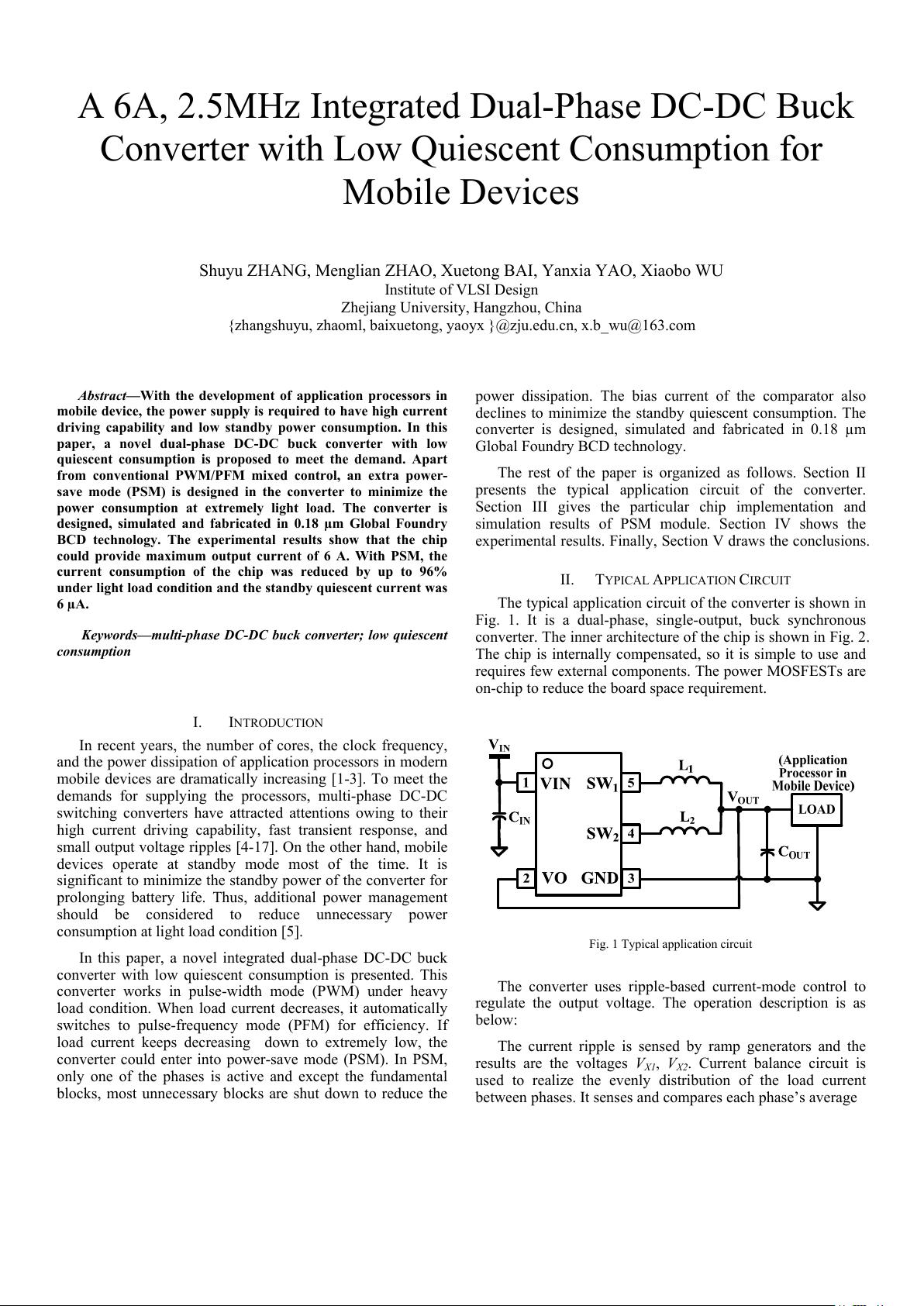
The typical application circuit of the converter is shown in
Fig. 1. It is a dual-phase, single-output, buck synchronous
converter. The inner architecture of the chip is shown in Fig. 2.
The chip is internally compensated, so it is simple to use and
requires few external components. The power MOSFESTs are
on-chip to reduce the board space requirement.
Fig. 1 Typical application circuit
The converter uses ripple-based current-mode control to
regulate the output voltage. The operation description is as
below:
The current ripple is sensed by ramp generators and the
results are the voltages V
X1
, V
X2
. Current balance circuit is
used to realize the evenly distribution of the load current
between phases. It senses and compares each phase’s average


