
© Semiconductor Components Industries, LLC, 2015
November, 2015 − Rev. 5
1 Publication Order Number:
NTMFS4C09N/D
NTMFS4C09N
Power MOSFET
30 V, 52 A, Single N−Channel, SO−8 FL
Features
• Low R
DS(on)
to Minimize Conduction Losses
• Low Capacitance to Minimize Driver Losses
• Optimized Gate Charge to Minimize Switching Losses
• These Devices are Pb−Free, Halogen Free/BFR Free and are RoHS
Compliant
Applications
• CPU Power Delivery
• DC−DC Converters
MAXIMUM RATINGS (T
J
= 25°C unless otherwise stated)
Parameter
Symbol Value Unit
Drain−to−Source Voltage V
DSS
30 V
Gate−to−Source Voltage V
GS
±20 V
Continuous Drain
Current R
q
JA
(Note 1)
Steady
State
T
A
= 25°C
I
D
16.4
A
T
A
= 80°C 12.3
Power Dissipation
R
q
JA
(Note 1)
T
A
= 25°C P
D
2.51 W
Continuous Drain
Current R
q
JA
≤ 10 s
(Note 1)
T
A
= 25°C
I
D
25.3
A
T
A
= 80°C 19.0
Power Dissipation
R
q
JA
≤ 10 s (Note 1)
T
A
= 25°C P
D
6.0 W
Continuous Drain
Current R
q
JA
(Note 2)
T
A
= 25°C
I
D
9.0
A
T
A
= 80°C 6.8
Power Dissipation
R
q
JA
(Note 2)
T
A
= 25°C P
D
0.76 W
Continuous Drain
Current R
q
JC
(Note 1)
T
C
= 25°C
I
D
52
A
T
C
=80°C 39
Power Dissipation
R
q
JC
(Note 1)
T
C
= 25°C P
D
25.5 W
Pulsed Drain
Current
T
A
= 25°C, t
p
= 10 ms
I
DM
146 A
Current Limited by Package T
A
= 25°C I
Dmax
80 A
Operating Junction and Storage
Temperature
T
J
,
T
STG
−55 to
+150
°C
Source Current (Body Diode) I
S
23 A
Drain to Source dV/dt dV/d
t
7.0 V/ns
Single Pulse Drain−to−Source Avalanche
Energy (T
J
= 25°C, V
GS
= 10 V, I
L
= 29 A
pk
,
L = 0.1 mH, R
GS
= 25 W) (Note 3)
E
AS
42 mJ
Lead Temperature for Soldering Purposes
(1/8″ from case for 10 s)
T
L
260 °C
Stresses exceeding those listed in the Maximum Ratings table may damage the
device. If any of these limits are exceeded, device functionality should not be
assumed, damage may occur and reliability may be affected.
1. Surface−mounted on FR4 board using 1 sq−in pad, 1 oz Cu.
2. Surface−mounted on FR4 board using the minimum recommended pad size.
3. Parts are 100% tested at T
J
= 25°C, V
GS
= 10 V, I
L
= 20 A
pk
, EAS = 20 mJ.
MARKING
DIAGRAMS
www.onsemi.com
V
(BR)DSS
R
DS(ON)
MAX I
D
MAX
30 V
5.8 mW @ 10 V
52 A
8.5 mW @ 4.5 V
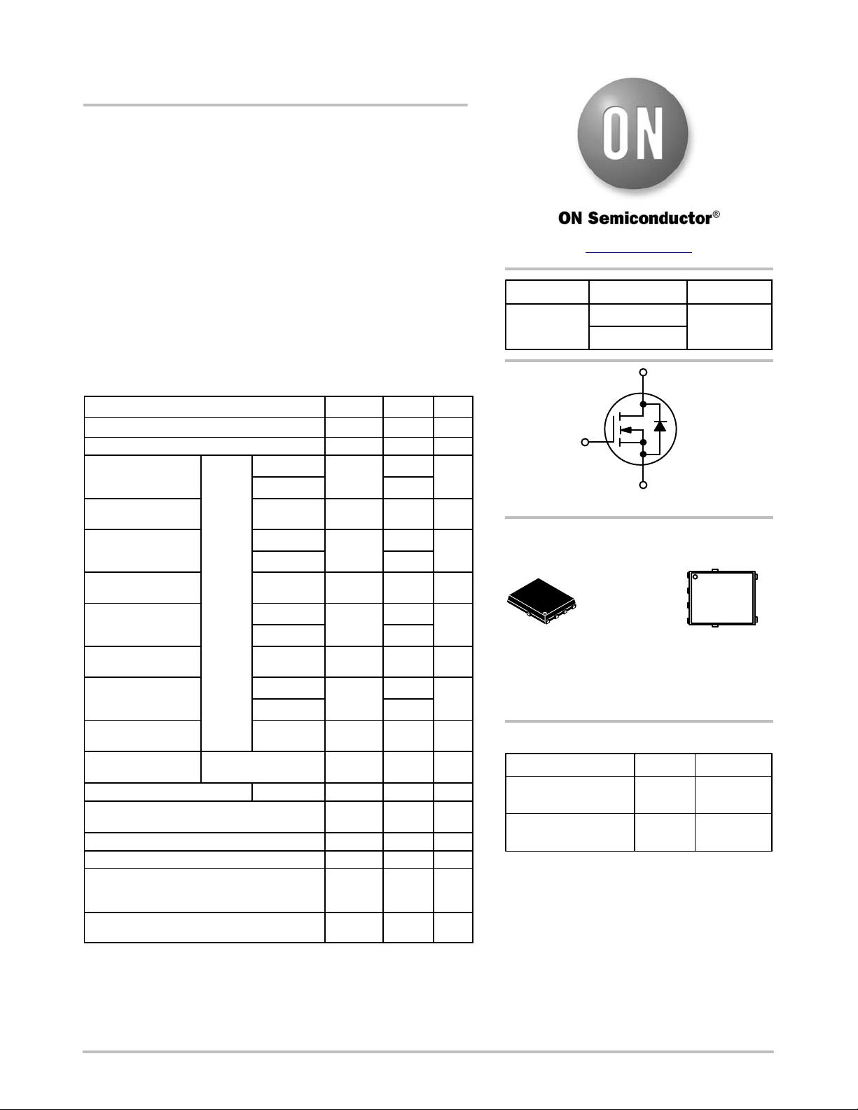
N−CHANNEL MOSFET
G (4)
S (1,2,3)
D (5−8)
SO−8 FLAT LEAD
CASE 488AA
STYLE 1
A = Assembly Location
Y = Year
W = Work Week
ZZ = Lot Traceabililty
4C09N
AYWZZ
1
Device Package Shipping
†
ORDERING INFORMATION
NTMFS4C09NT1G SO−8 FL
(Pb−Free)
1500 /
Tape & Reel
NTMFS4C09NT3G SO−8 FL
(Pb−Free)
5000 /
Tape & Reel
†For information on tape and reel specifications,
including part orientation and tape sizes, please
refer to our Tape and Reel Packaging Specification
s
Brochure, BRD8011/D.
S
S
S
G
D
D
D
D
下载后可阅读完整内容,剩余6页未读,立即下载

LC灵灵
- 粉丝: 1
- 资源: 261
 我的内容管理
展开
我的内容管理
展开


最新资源
- C++标准程序库:权威指南
- Java解惑:奇数判断误区与改进方法
- C++编程必读:20种设计模式详解与实战
- LM3S8962微控制器数据手册
- 51单片机C语言实战教程:从入门到精通
- Spring3.0权威指南:JavaEE6实战
- Win32多线程程序设计详解
- Lucene2.9.1开发全攻略:从环境配置到索引创建
- 内存虚拟硬盘技术:提升电脑速度的秘密武器
- Java操作数据库:保存与显示图片到数据库及页面
- ISO14001:2004环境管理体系要求详解
- ShopExV4.8二次开发详解
- 企业形象与产品推广一站式网站建设技术方案揭秘
- Shopex二次开发:触发器与控制器重定向技术详解
- FPGA开发实战指南:创新设计与进阶技巧
- ShopExV4.8二次开发入门:解决升级问题与功能扩展
资源上传下载、课程学习等过程中有任何疑问或建议,欢迎提出宝贵意见哦~我们会及时处理!
点击此处反馈


