AN920/D
http://onsemi.com
8
5. The peak switch current is:
I
pk(switch)
+ 2I
out
+ 2(50 10
−3
)
+ 100 mA
6. With knowledge of the peak switch current and
maximum on time, a minimum value of inductance
can be calculated.
L
min
+
ǒ
V
in(min)
* V
sat
* V
out
I
pk(switch)
Ǔ
t
on(max)
+
ǒ
21.6 * 0.8 * 5.0
100 10
−3
Ǔ
5.4 10
−6
+ 853 mH
7. A value for the current limit resistor, R
sc
, can be
determined by using the current level of I
pk(switch)
when V
in
= 24 V.
IȀ
pk(switch)
+
ǒ
V
in
* V
sat
* V
out
L
min
Ǔ
t
on(max)
+
ǒ
24 * 0.8 * 5.0
853 10
−6
Ǔ
5.4 10
−6
+ 115 mA
R
sc
+
0.33
IȀ
pk(switch)
+
0.33
115 10
−3
+ 2.86 W ,use2.7W
This value may have to be adjusted downward to
compensate for conversion losses and any increase
in I
pk(switch
) current if V
in
varies upward. Do not set
R
sc
to exceed the maximum I
pk(switch)
limit of 1.5 A
when using the internal switch transistor.
8. A minimum value for an ideal output filter capacitor
can now be obtained.
C
o
+
I
pk(switch)
(t
on
) t
off
)
8V
ripple(p−p)
+
0.1 (20 10
−6
)
8(25 10
−3
)
+ 10 mF
Ideally this would satisfy the design goal, however,
even a solid tantalum capacitor of this value will
have a typical ESR (equivalent series resistance) of
0.3 Ω which will contribute 30 mV of ripple. The
ripple components are not in phase, but can be
assumed to be for a conservative design. In
satisfying the example shown, a 27 μF tantalum with
an ESR of 0.1 Ω was selected. The ripple voltage
should be kept to a low value since it will directly
affect the system line and load regulation.
9. The nominal output voltage is programmed by the
R1, R2 resistor divider. The output voltage is:
V
out
+ 1.25
ǒ
R2
R1
) 1
Ǔ
The divider current can go as low as 100 μA without
affecting system performance. In selecting a
minimum current divider R1 is equal to:
R1 +
1.25
100 10
−6
+ 12, 500 W
Rearranging the above equation so that R2 can be
solved yields:
R2 + R1
ǒ
V
out
1.25
* 1
Ǔ
If a standard 5% tolerance 12 k resistor is chosen for
R1, R2 will also be a standard value.
R2 + 12 10
3
ǒ
5.0
1.25
* 1
Ǔ
+ 36 k
Using the above derivation, the design is optimized to
meet the assumed conditions. At V
in(min)
, operation is at the
onset of continuous mode and the output current capability
will be greater than 50 mA. At V
in(nom)
i.e., 24 V, the current
limit will activate slightly above the rated I
out
of 50 mA.
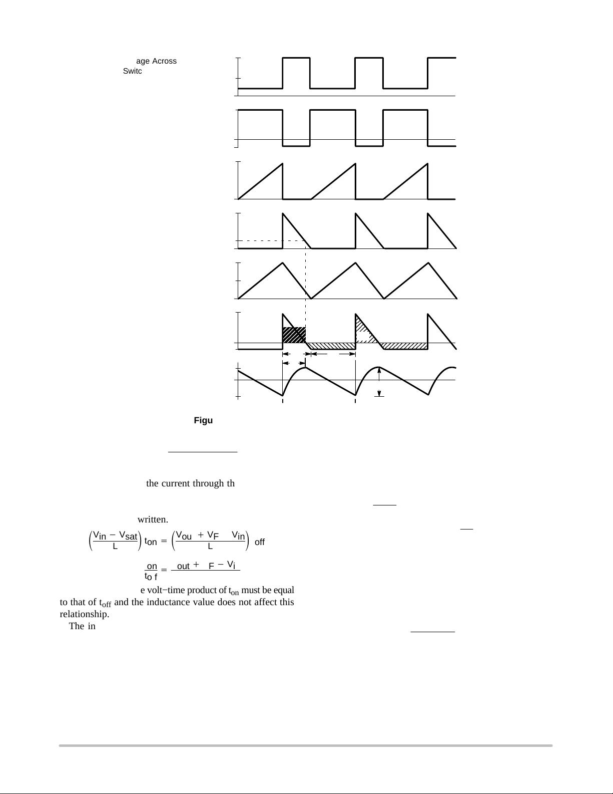
STEP−UP SWITCHING REGULATOR OPERATION
The basic step−up switching regulator is shown in Figure
7b and the waveform is in Figure 10. Energy is stored in the
inductor during the time that transistor Q1 is in the “on”
state. Upon turn−off, the energy is transferred in series with
V
in
to the output filter capacitor and load. This configuration
allows the output voltage to be set to any value greater than
that of the input by the following relationship:
V
out
+ V
in
ǒ
t
on
t
off
Ǔ
) V
in
or V
out
+ V
in
ǒ
t
on
t
off
) 1
Ǔ
An explanation of the step−up converter’s operation is as
follows. Initially, assume that transistor Q1 is off, the
inductor current is zero, and the output voltage is at its
nominal value. At this time, load current is being supplied
only by C
o
and it will eventually fall below nominal. This
deficiency will be sensed by the control circuit and it will
initiate an on−cycle, driving Q1 into saturation. Current will
start to flow from V
in
through the inductor and Q1 and rise
at a rate of ΔI/ΔT = V/L. The voltage across the inductor is
equal to V
in
− V
sat
and the peak current is:
I
L
+
ǒ
V
in
* V
sat
L
Ǔ
t
When the on−time is completed, Q1 will turn off and the
magnetic field in the inductor will start to collapse
generating a reverse voltage that forward biases D1,
supplying energy to C
o
and R
L
. The inductor current will
decay at a rate of ΔI/ΔT = V/L and the voltage across it is
equal to V
out
+ V
F
− V
in
. The current at any instant is:


