


MT7976CNDatasheet:详解802.11ax Wi-Fi RF 芯片中文版规格
需积分: 24 8 浏览量
更新于2024-06-26
收藏 1.53MB PDF 举报
联发科MT7976芯片手册中文版是一份详细的规格文档,针对的是802.11ax Wi-Fi无线通信RF芯片。该芯片由联发科公司开发,适用于那些需要高性能、高效能的Wi-Fi解决方案的设备制造商。手册的最新版本为1.2,发布于2021年11月15日,由TM Chen进行修订。
在文档的"系统概述"部分,用户可以找到芯片的功能块图解,这有助于理解各部件之间的相互作用和系统架构。MT7976CNDatasheet提供了丰富的功能特性,包括可能支持的Wi-Fi标准(如802.11ac和802.11ax),这表明它是一款高度集成的解决方案,旨在提供高速数据传输和低延迟。
"Pin Definitions"和"Pin Layout"章节详细列出了芯片的所有引脚定义和布局,这对于硬件工程师在设计和集成MT7976芯片时至关重要。这些信息包括每个引脚的电气特性、功能以及连接器配置,确保了电路板设计的正确性和兼容性。
"Electrical Characteristics"部分包括了芯片的极限操作条件和推荐工作范围,帮助工程师了解如何在安全的条件下使用该芯片,以防止过载或损坏。此外,还提供了电源供应规格,如电压范围和电流消耗,这对于优化功耗和散热管理非常重要。
"Digital Logic Characteristics"部分则深入探讨了芯片内部逻辑单元的工作原理和性能指标,如时钟速度、接口规范等,对于软件开发者理解和编程芯片的行为具有指导意义。
MT7976CNTOP Building Blocks章节可能是芯片的高级模块介绍,可能涵盖了Wi-Fi通信子系统的各个组件,如调制解调器、天线管理、MAC和PHY层,这些对于Wi-Fi功能实现的关键部分进行了详细阐述。
最后,手册还可能包含关于晶振(XO)和启动器电路(Bootstrap)的设计指南,这些都是实现无线通信稳定性和精确频率同步的重要部分。
联发科MT7976芯片手册中文版为开发人员提供了全面的参考,无论是硬件设计还是软件开发,都不可或缺。通过这份手册,工程师能够深入了解芯片的性能限制、电气参数,以及如何正确配置和驱动MT7976,从而打造出高质量的Wi-Fi产品。
loginid=jiangkejun@cmdc.chinamobile.com,time=2022-03-17 19:18:21,ip=120.229.34.168,doctitle=MT7976CN_Datasheet_1.2.pdf,company=
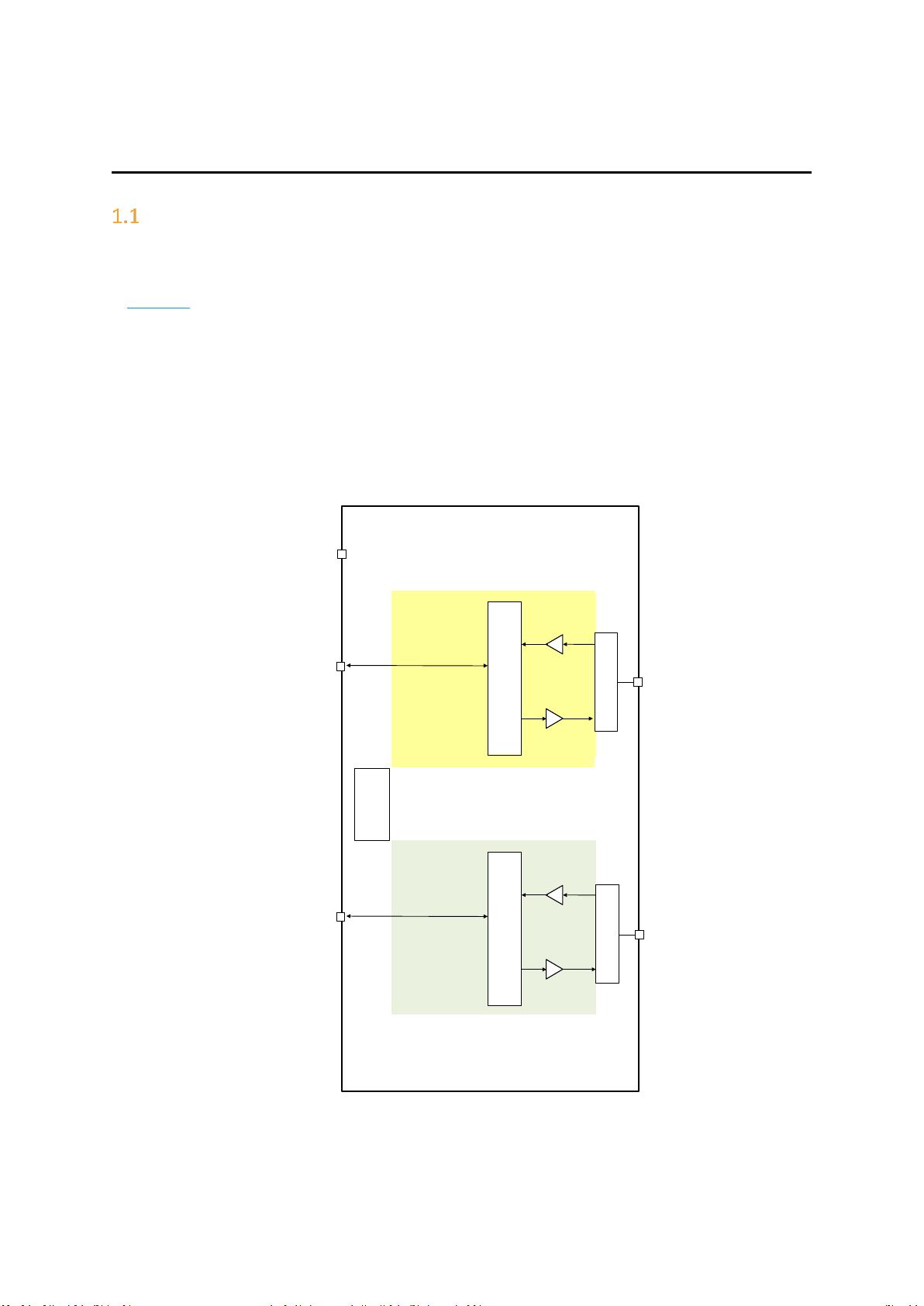
1 System Overview
Functional Block Diagram
MT7976CN is an IEEE WiFi 6 MIMO RF chip which contains 2.4 GHz WI-Fi transceiver front-ends and 5 GHz Wi-
Fi transceiver front-ends in a DRQFN package. Simplified block diagram and how MT7976CN is used are shown
in Figure 1-1. The top control logics control each subsystem independently. Each subsystem also has dedicated
LDOs. A thermal sensor and a low-speed ADC (Analog-to-Digital Converter) are provided to monitor
MT7976CN’s temperature variation. MT7976CN have its dedicated crystal oscillator (XO) circuit. Besides, XO
circuit provides an external clock source to other chips in the platform.
The transceiver front-ends are on MT7976CN while the ADC/DAC (Analog-to-Digital Converter/Digital-to-
Analog Converter) is in the companion modem chip. The interface drivers/receiver buffers are designed to
drive PCB trace loading.
Figure 1-1. MT7976CN block diagram
XO IN
MT7976CN
WiFi_2G
Tx/ Rx IQ
5 G RF
TRx
5 G WiFi RF
2G RFIO
LNA
5 G RF
TRx
5 G WiFi RF
LNA
5 G RF
TRx
5 G WiFi RF
LNA
WIFI
2G WiFi RF
LNA
PA
WiFi_5G
Tx/ Rx IQ
5 G RF
TRx
5 G WiFi RF
5G RFIO
LNA
5 G RF
TRx
5 G WiFi RF
LNA
5 G RF
TRx
5 G WiFi RF
LNA
WIFI
5G WiFi RF
LNA
PA
3- wire
Ctrl
3- wire
Ctrl
3- wire
Ctrl
3- wire
Ctrl
TRSW
TRSW
下载后可阅读完整内容,剩余22页未读,立即下载
1045 浏览量
180 浏览量
228 浏览量
点击了解资源详情
点击了解资源详情
点击了解资源详情
1667 浏览量
1520 浏览量
2208 浏览量


CookieAndCat
- 粉丝: 0
 我的内容管理
展开
我的内容管理
展开


最新资源
- 使用echarts绘制石家庄地图数据可视化的实践
- UFO档案文章系统源码下载
- Megalui:探索基于GLUI的科学可视化库
- Win7 x32/x64下Delphi帮助文件无法打开的解决方法
- DELPHI实现对PowerPoint的自动化控制教程
- CSS+DIV实例素材下载:提升网页设计技能
- Vapor:Node.js轻量级Steam客户端框架的探索
- STM32F2系列深入培训资料
- JavaScript/CSS Reset工具类封装总结
- 基于JSP的简易银行柜员系统开发教程
- FAO-56推荐cropwat8.0软件:计算作物需水量
- Android浏览器源码的下载与修改技巧
- C#实现的电影票在线售票系统Mycinema功能全解析
- Chewie的宠物日常习惯追踪客户端应用
- GX Developer 8.52 中文版:三菱PLC编程软件使用体验
- C语言编写的编译原理词法分析器详解