Ublox LEA-6/NEO-6 GPS模块集成手册:高性价比设计指南
本指南深入探讨了Ublox LEA-6和NEO-6系列GPS模块的设计细节,特别针对硬件工程师而言,具有极高的实用价值。Ublox是一家专注于高性价比且性能卓越的GPS模块制造商,其LEA-6和NEO-6模块集成了u-blox 6定位引擎,展现出出色的导航能力。这些模块设计紧凑,易于集成,是独立式GPS接收器的理想选择。
LEA-6和NEO-6模块的特点在于它们的高度灵活性,支持多种电源选项,让设计师在满足不同应用需求的同时,兼顾功耗和成本效益。它们的SMT(表面安装技术)封装使得自动化组装成为可能,无论是标准的拾取和放置机器还是回流焊设备,都能高效完成大规模生产,从而大大缩短产品上市时间。
此外,文档还强调了这些模块在定位、通信和加速方面的功能,旨在帮助用户迅速准确地定位设备位置,并通过内置的AGPS(辅助全球定位系统)增强定位精度,确保在城市峡谷或其他信号较弱地区也能提供稳定的定位服务。值得注意的是,文档中提供的信息基于早期版本,后续可能会有修订和补充内容发布,因此建议读者在实际操作前参考最新的官方资料。
LEA-6/NEO-6 GPS模块设计指南提供了详尽的技术参数、接口规范以及集成指南,对于硬件工程师在项目开发过程中选择和优化GPS解决方案具有重要的参考价值。通过了解和遵循这份手册,硬件工程师可以充分利用Ublox的先进技术,实现高效、可靠的GPS定位应用设计。

LEA-6 / NEO-6 - Hardware Integration Manual
GPS.G6-HW-09007-A Preliminary Hardware description
Page 11 of 62
The Power Save mode is an autonomous mode that does not require dynamic interaction by the application
engine, i.e. after the configuration settings communicated to the u-blox 6 receiver, the application does not
need to take care of switching off and on the receiver to obtain low power consumption.
With NEO-6G the Power Save Mode does not achieve lowest possible current during backup mode (SW backup
current). This leads to reduced power savings only for the combination of very long off-times (several hours) and
1.8 V supply. For this scenario, better current savings can be achieved if the Module is externally turned off.
Please refer to the u-blox 6 Receiver Description including Protocol Specification [3] for more information. This
document is available on the
ublox website.
Power Save mode is not available with LEA-6R.
1.4 Antenna supply - V_ANT (LEA-6)
LEA-6 modules support active antenna supply and supervision use the pin V_ANT to supply the active antenna.
Use a 10R resistor in front of V_ANT. For more information about antenna and antenna supervisor see chapter
2.5.
1.5 System functions
1.5.1 EXTINT - External interrupt pin
EXTINT0 is an external interrupt pin used for the time mark function on LEA-6T.
It can be used for wake-up functions in Power Save mode on all LEA-6 and NEO-6 modules.
1.5.2 System monitoring
The u-blox-6 receiver modules provide system monitoring functions that allow the operation of the embedded
processor and associated peripherals to be supervised. These System Monitoring functions are output as part of
the UBX protocol, class ‘MON’.
Please refer to the u-blox 6 Receiver Description including Protocol Specification [3]. For more information on
UBX messages, serial interfaces for design analysis and individual system monitoring functions.
1.6 Interfaces
1.6.1 UART
u-blox 6 modules include a Universal Asynchronous Receiver Transmitter (UART) serial interface. RxD1/TxD1
supports data rates from 4.8 to 230.4 kBit/s. The signal output and input levels are 0 V to VCC. An interface
based on RS232 standard levels (+/- 12 V) can be realized using level shifters such as Maxim MAX3232.
Hardware handshake signals and synchronous operation are not supported.
For the default settings see the module data sheet.
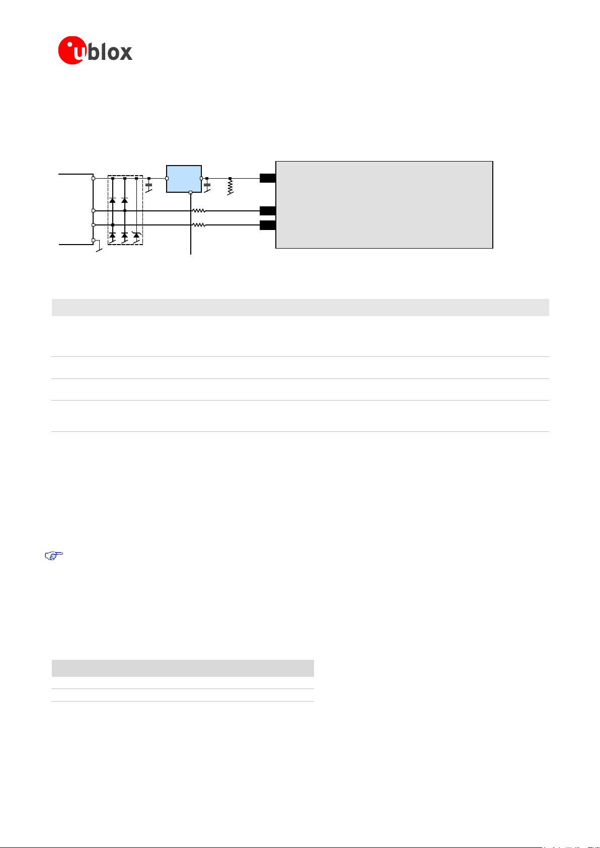
1.6.2 USB
The u-blox 6 Universal Serial Bus (USB) interface supports the full-speed data rate of 12 Mbit/s.
1.6.2.1 USB external components
The USB interface requires some external components in order to implement the physical characteristics required
by the USB 2.0 specification. These external components are shown in Figure 4 and listed in Table 1.
In order to comply with USB specifications, VBUS must be connected through a LDO (U1) to pin VDD_USB of
the module.
If the USB device is self-powered it is possible that the power supply (VCC) is shut down and the Baseband-IC
core is not powered. Since VBUS is still available, it still would be signaled to the USB host that the device is
present and ready to communicate. This is not desired and thus the LDO (U1) should be disabled using the
剩余61页未读,继续阅读
1093 浏览量
306 浏览量
312 浏览量
点击了解资源详情
点击了解资源详情
点击了解资源详情
315 浏览量

汉码盘点机PDA
- 粉丝: 49
- 资源: 9
 我的内容管理
展开
我的内容管理
展开


最新资源
- Apache Kafka的Python客户端-Python开发
- matlab_code:与论文相关的一些代码
- lean-intl:Lean-Intl是针对尚不支持此API的浏览器的Intl-API的精益polyfill。 这是Intl.js的现代分支,具有最新数据,已根据现代开发工作流程和工具要求进行了调整
- 一组dashboard仪表盘图标 .svg .png素材下载
- 易语言多彩文本
- 浅析屏蔽电缆的接地方式.rar
- LengthConverter:该长度转换器应用程序将给定的长度(以米为单位)转换为毫米,厘米,英寸,英尺,码,公里等。此应用程序是使用HTML,CSS,BOOTSTRAP,JAVASCRIPT开发的
- laravel引入自定义composer包文件.zip
- jdbc-jar,数据库连接驱动,三个jar包。包括druid连接池,ojdbc1.6,lombok。
- PokemonApp:应用程序列出宠物小精灵
- QT5网络通讯TCP服务器端代码,linux和win兼容,亲测可用
- 单目标动态发电调度粒子群算法,c语言档案管理界面的源码,c语言
- 使用Arduino和环氧树脂制作的夜灯-电路方案
- Playwright是一个Python库,可通过单个API自动化Chromium,Firefox和WebKit浏览器-Python开发
- 气旋物理学:《游戏物理引擎设计》一书随附的物理引擎
- homebrew-pythons::beer_mug::snake:一个Hombrew Tap,字面上充满了Python解释器
