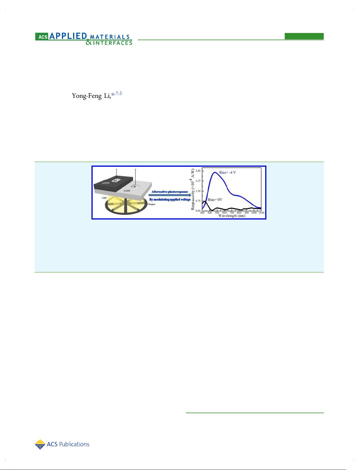
Alternative Spectral Photoresponse in a p‑Cu
2
ZnSnS
4
/n‑GaN
Heterojunction Photodiode by Modulating Applied Voltage
Gang Yang,
†
Yong-Feng Li,*
,†,‡
Bin Yao,*
,†,‡
Zhan-Hui Ding,
†
Rui Deng,
§
Xuan Fang,
∥
and Zhi-Peng Wei
∥
†
State Key Lab of Superhard Materials and College of Physics, Jilin University, Changchun 130012, People’s Republic of China
‡
Key Laboratory of Physics and Technology for Advanced Batteries (Ministry of Education), College of Physics, Jilin University,
Changchun 130012, China
§
School of Materials Science and Engineering, Changchun University of Science and Technology, Changchun 130022, China
∥
State Key Laboratory on High-Power Semiconductor Lasers, Changchun University of Science and Technology, 7186 Wei-Xing
Road, Changchun 130022, China
ABSTRACT: We report alternative visible and ultraviolet light response spectra in a p-Cu
2
ZnSnS
4
(p-CZTS)/n-GaN
heterojunction photodiode. A CZTS film was deposited on an n-GaN/sapphire substrate using a magnetron sputtering method.
Current−voltage characteristic of the p-CZTS/n-GaN heterojunction photodiode showed a good rectifying behavior. The
spectral response measurements indicate that the response wavelength of the photodiode can be tuned from ultraviolet to visible
regions via applying zero and reverse bias. A band alignment at the interface of the p-CZTS/n-GaN heterojunction was proposed
to interpret the spectral response of the device.
KEYWORDS: photodiode, GaN, magnetron sputtering, Cu
2
ZnSnS
4
, heterojunction
■
INTRODUCTION
Solar energy is considered to be the most economic and
effective available renewable energy resources.
1−3
Photovoltaic
(PV) cells including thin film solar cells,
4
dye-sensitized solar
cells,
5
organic bulk junction solar cells,
6
and hybrid perovskite
solar cells
7,8
have been widely investigated because they can
convert sunlight directly into electricity. In recent years, the
kesterite Cu
2
ZnSnS
4
(CZTS) emerged as a potential p-type
material used in thin film photovoltaic applications.
9−12
It has
an ideal direct bandgap of about 1.5 eV and a large absorption
coefficient (>10
4
cm
−1
).
13,14
The use of only nontoxic and
abundant elements makes it to be more environmental friendly
and economical compared with CdTe and Cu(In
1−x
Ga
x
)-
Se
2.
15,16
Recently, various deposition techniques including
vacuum and nonvacuum methods were applied to fabricate
CZTS solar cells, and the power conversion efficiency (PCE)
record has been updated rapidly.
17−19
A typical structure of CZTS solar cells is Mo/CZTS/CdS/
ZnO/ZnO:Al/Al.
11
The n-type CdS buffer layer is fabricated
on the p-type CZTS absorption layer to form a p−n junction,
where carriers are separated as light irradiates. The wide
bandgap semiconductors including an intrinsic ZnO and a
heavily n-doped ZnO:Al were usually used as the window layer,
which reduces the series resistance of solar cells.
20
Recently,
researches also focused on direct deposition of n-type wide-
bandgap ZnO on p-type CZTS to form Cd-free p-CZTS/n-
ZnO heterojunction devices.
21,22
Htay et al. reported the higher
open circuit voltage (V
oc
) and relative quantum efficiency at the
short wavelength regions in the p-CZTS/n-ZnO heterojunction
solar cells than those using CdS as the buffer layer.
23
They
ascribed these to the higher built-in potential induced by the
wider bandgap ZnO and the increase of transparency. In
addition, the proposed type-I band alignment of CZTS/ZnO
heterojunction (i.e., the conduction band of CZTS is lower
than that of ZnO) can reduce the recombination rate greatly.
Among lots of wide-bandgap semiconductors, gallium nitride
(GaN) has the same wurtzite structure with ZnO and similar
wide direct bandgap (3.4 eV).
24,25
But few reports were
available for the CZTS/GaN heterojunction. Due to the
advantages of high saturation velocity (2.7 × 10
7
cm/s),
radiation hardness, tolerability of aggressive environments, and
a more mature processing technique, GaN was widely used for
fabricating photodetectors.
26−28
More importantly, the type-I
band alignment of the CZTS/GaN interface with a small
Received: May 17, 2015
Accepted: July 16, 2015
Published: July 16, 2015
Research Article
www.acsami.org
© 2015 American Chemical Society 16653 DOI: 10.1021/acsami.5b04287
ACS Appl. Mater. Interfaces 2015, 7, 16653−16658


