16
DS90UH940N-Q1
ZHCSIG6A –JULY 2018–REVISED OCTOBER 2018
www.ti.com.cn
Copyright © 2018, Texas Instruments Incorporated
Switching Characteristics (continued)
Over recommended operating supply and temperature ranges unless otherwise specified.
PARAMETER TEST CONDITIONS PIN/FREQ. MIN TYP MAX UNIT
(2) a. 1280 × 720p60; PCLK = 74.25 MHz; 4 MIPI lanes Reg0x6C = 0x02; Reg0x6D = 0x84
b. 1280 × 720p60; PCLK = 74.25MHz; 2 MIPI lanes Reg0x6C = 0x02; Reg0x6D = 0x89
c. 640 × 480p60; PCLK = 25 MHz; 4 MIPI lanes Reg0x6C = 0x02; Reg0x6D = 0x82
d. 640 × 480p60; PCLK = 25 MHz; 2 MIPI lanes Reg0x6C = 0x02; Reg0x6D = 0x83
e. Other video formats may require additional register configuration.
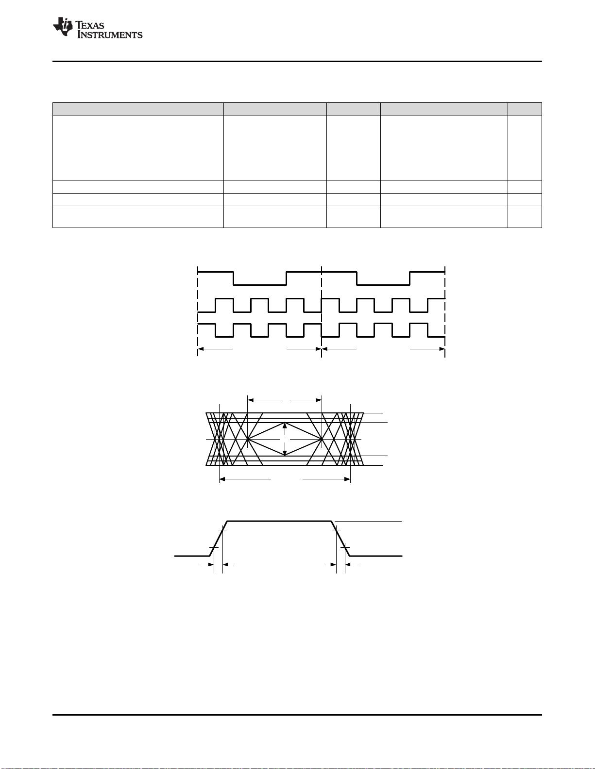
DATA-CLOCK TIMING SPECIFICATIONS (图图 10)
UI
INST
UI instantaneous
f
CLK
= CSI-2 DDR clock
frequency
CSI0_D0±
CSI0_D1±
CSI0_D2±
CSI0_D3±
CSI1_D0±
CSI1_D1±
CSI1_D2±
CSI1_D3±
CSI0_CLK±
CSI1_CLK±
1/(f
CLK
× 2)
UI
ΔUI UI variation
UI ≥ 1 ns –10% 10% UI
UI < 1 ns –5% 5% UI
t
SKEW(TX)
Data to clock skew (measured at
transmitter)
Skew between clock and data
from ideal center
Data rate ≤ 1 Gbps –0.15 0.15 UI
INST
Data rate > 1 Gbps –0.2 0.2 UI
INST
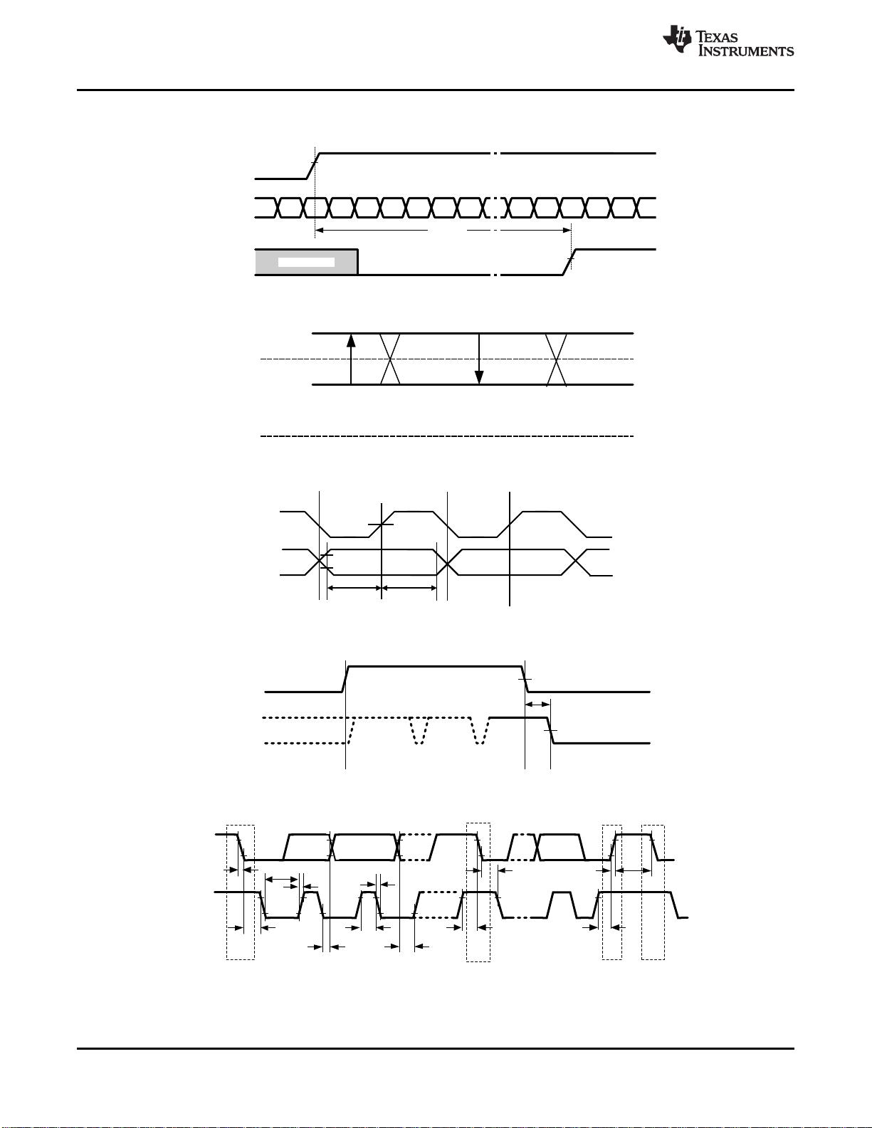
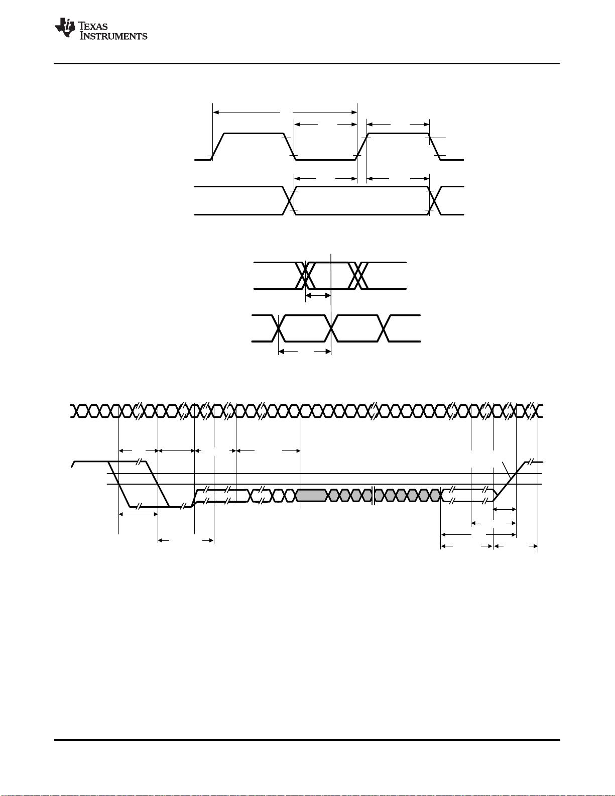
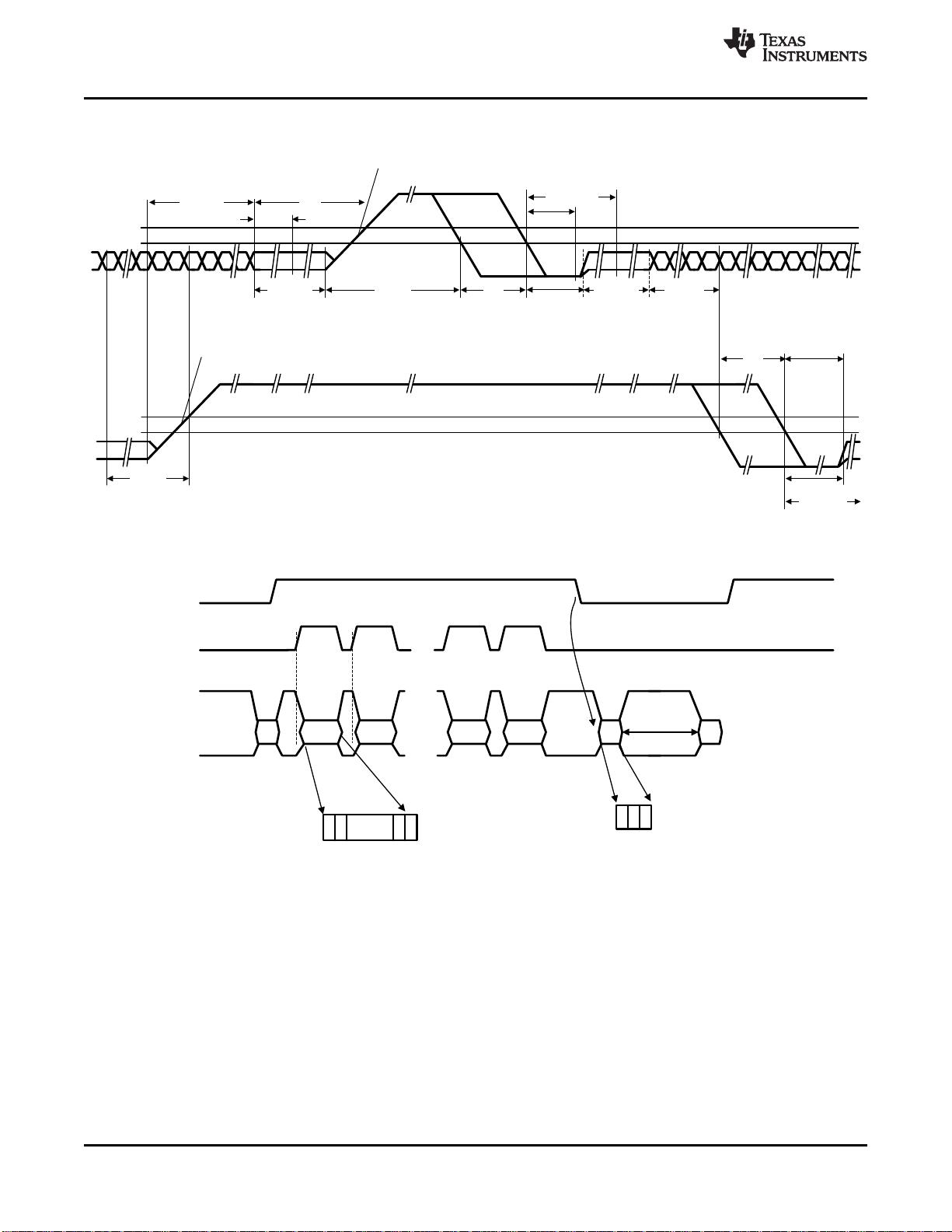
CSI-2 TIMING SPECIFICATIONS (图图 11, 图图 12)
t
CLK-MISS
Timeout for receiver to detect
absence of clock transitions and
disable the clock lane HS-RX
CSI0_D0±
CSI0_D1±
CSI0_D2±
CSI0_D3±
CSI1_D0±
CSI1_D1±
CSI1_D2±
CSI1_D3±
CSI0_CLK±
CSI1_CLK±
60 ns
t
CLK-POST
HS exit 60 + 52 × UI ns
t
CLK-PRE
Time HS clock shall be driver
prior to any associated data lane
beginning the transition from LP
to HS mode
8 UI
t
CLK-
PREPARE
Clock lane HS Entry 38 95 ns
t
CLK-SETTLE
Time interval during which the
HS receiver shall ignore any
clock lane HS transitions
95 300 ns
t
CLK-TERM-EN
Timeout at clock lane display
module to enable HS Termination
Time for Dn to
reach VTERM-
EN
38 ns
t
CLK-TRAIL
Time that the transmitter drives
the HS-0 state after the last
payload clock bit of a HS
transmission burst
60 ns
t
CLK-
PREPARE
+
t
CLK-ZERO
TCLK-PREPARE + time that the
transmitter drives the HS-0 state
prior to starting the Clock
300 ns
t
D-TERM-EN
Time for the Data Lane receiver
to enable the HS line termination
Time for Dn to
reach V-
TERM-EN
35 + 4
× UI
ns
t
EOT
Transmitted time interval from the
start of t
HS-TRAIL
to the start of the
LP-11 state following a HS burst
see
(2)
105 +
12 × UI
ns
t
HS-EXIT
Time that the transmitter drives
LP=11 following a HS burst
100 ns
t
HS-PREPARE
Data lane HS entry 40 + 4 × UI
85 + 6
× UI
ns
t
HS-PREPARE
+ t
HS-ZERO
t
HS-PREPARE
+ time that the
transmitter drives the HS-0 state
prior to transmitting the sync
sequence
145 + 10 × UI ns
t
HS-SETTLE
Time interval during which the
HS receiver ignores any data
lane HS transitions, starting from
the beginning of t
HS-SETTLE
85 + 6 × UI
145 +
10 × UI
ns


