t
ON
t
OFF
[LEDx_PKTH_DAC]
and R
SENSE
adjust
the peak inductor
current
The Inductance (L)
and t
OFF
define 'I
L-PP
The average output current =
the peak ± ½ the peak to peak
inductor ripple
t
L(pk)
SENSE
[LEDx _PKTH _DAC]
I
1000* R
AVE
L PP
L LED L(pk)
I
I I I
2
'
12
TPS92518
SLUSCR7 –MAY 2017
www.ti.com
Product Folder Links: TPS92518
Submit Documentation Feedback Copyright © 2017, Texas Instruments Incorporated
8.3 Feature Description
8.3.1 General Operation
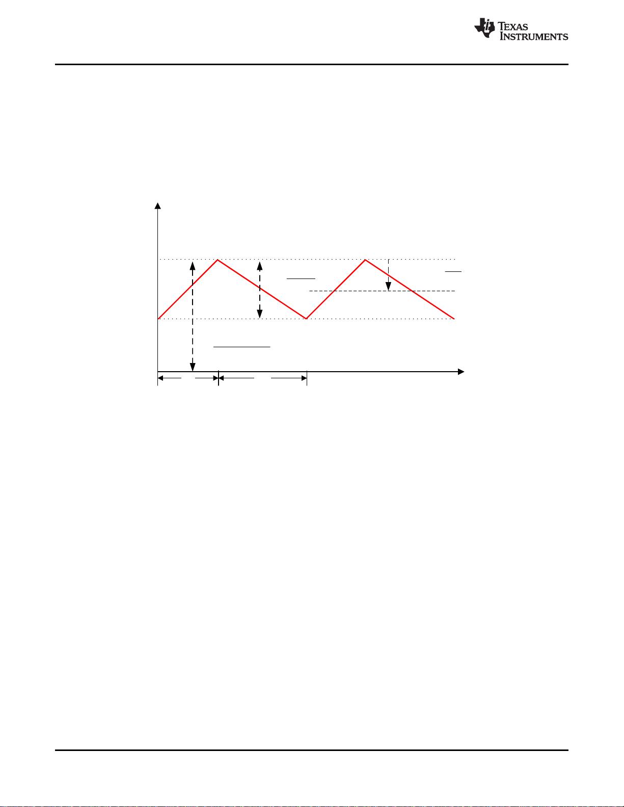
The TPS92518 operates using a peak-current, constant off-time control as described in Figure 16 . Two states
dictate the high-side FET control. The switch turns on and stays on until the programmed peak current is
reached. The peak current is controlled by monitoring the voltage across the sense resistor. When the voltage
drop is higher than the programmed threshold, the peak current is reached. The switch is then turned OFF,
which initiates an off-time period. An internal capacitor is then charged by a current source which varies in
relation to the VLEDx pin voltage. When the capacitor voltage reaches the DAC controlled threshold, the off-time
ends. The off-time capacitor resets and the main switch turns ON, starting the next ON cycle.
Figure 16. Hysteretic Operation
8.3.1.1 Constant Off-Time vs. Constant µs×V operation
Although commonly referred to as constant off-time, the off-time does vary with the output voltage in the standard
TPS92518 configuration. This relation ensures constant peak-to-peak inductor current ripple (ΔI
L-PP
). Although
not common, the VLEDx pin can be set to a fixed value to generate a truly constant off-time and limit changes in
frequency, however current regulation degrades. To maintain regulation and a constant ripple over various output
voltages, the converter off-time must become shorter or longer as VLEDx pin voltage changes. This results in a
change in frequency. In this regard, the off-time register can be considered as a seconds-times-volts setting (s ×
V) for the converter. The TPS92518 Electrical Characteristics table specification for off-time specifies a certain off
time duration for a certain register value. The time is also dependent on the VLEDx pin voltage. For example, the
off-time is specified at 4 µs for a V
VLEDx
= 30 V and LEDx_TOFF_DAC = 255. The internal analog circuitry
operates to keep the ripple and µs·V (micro-second volt) product constant. If the LEDx voltage changes to 15 V,
the off time adjusts to 8 µs. If the LEDx voltage changes to 60 V the off time adjusts to 2 µs, and so on.
Two general cases can be examined: If the input voltage and output voltage are relatively constant, the
frequency also remains constant. If either the input voltage or the output voltage changes, the frequency
changes. For a fixed input voltage, the device operates at the maximum frequency at 50% duty cycle and the
frequency reduces as the duty cycle becomes shorter or longer. A graphical representation is shown in
Figure 17.
For a fixed output voltage (V
VLEDx
), the off-time stays fixed. The frequency then increases as the duty cycle
becomes smaller with an increasing VIN voltage. This relation is shown in Figure 18.


