1998 May 15 12
Philips Semiconductors Product specification
Enhanced Video Input Processor (EVIP) SAA7111A
The output data formats are controlled via the I
2
C-bus bits
OFTS0, OFTS1 and RGB888. Timing for the data stream
formats, YUV (4 : 1 : 1) (12-bit), YUV (4 : 2 : 2) (16-bit),
RGB (5, 6 and 5) (16-bit) and RGB (8, 8 and 8) (24-bit)
with an LLC2 data rate, is achieved by marking each
second positive rising edge of the clock LLC in conjunction
with CREF (clock reference) (except RGB (8, 8 and 8),
see special application in Fig.32). The higher output
signals VPO15 to VPO8 in the YUV format perform the
digital luminance signal. The lower output signals
VPO7 to VPO0 in the YUV format are the bits of the
multiplexed colour difference signals (B − Y) and (R − Y).
The arrangement of the RGB (5, 6 and 5) and
RGB (8, 8 and 8) data stream bits on the VPO-bus is given
in Table 6.
The data stream format YUV 4:2:2 (the 8 higher output
signals VPO15 to VPO8) in LLC data rate fulfils the
CCIR-656 standard with its own timing reference code at
the start and end of each video data block.
A pixel in the format tables is the time required to transfer
a full set of samples. If 16-bit 4 : 2 : 2 format is selected
two luminance samples are transmitted in comparison to
one (B − Y) and one (R − Y) sample within a pixel.
The time frames are controlled by the HREF signal.
Fast enable is achieved by setting input FEI to LOW.
The signal is used to control fast switching on the digital
VPO-bus. HIGH on this pin forces the VPO outputs to a
high-impedance state (see Figs 18 and 19). The I
2
C-bus
bit OEYC has to be set HIGH to use this function.
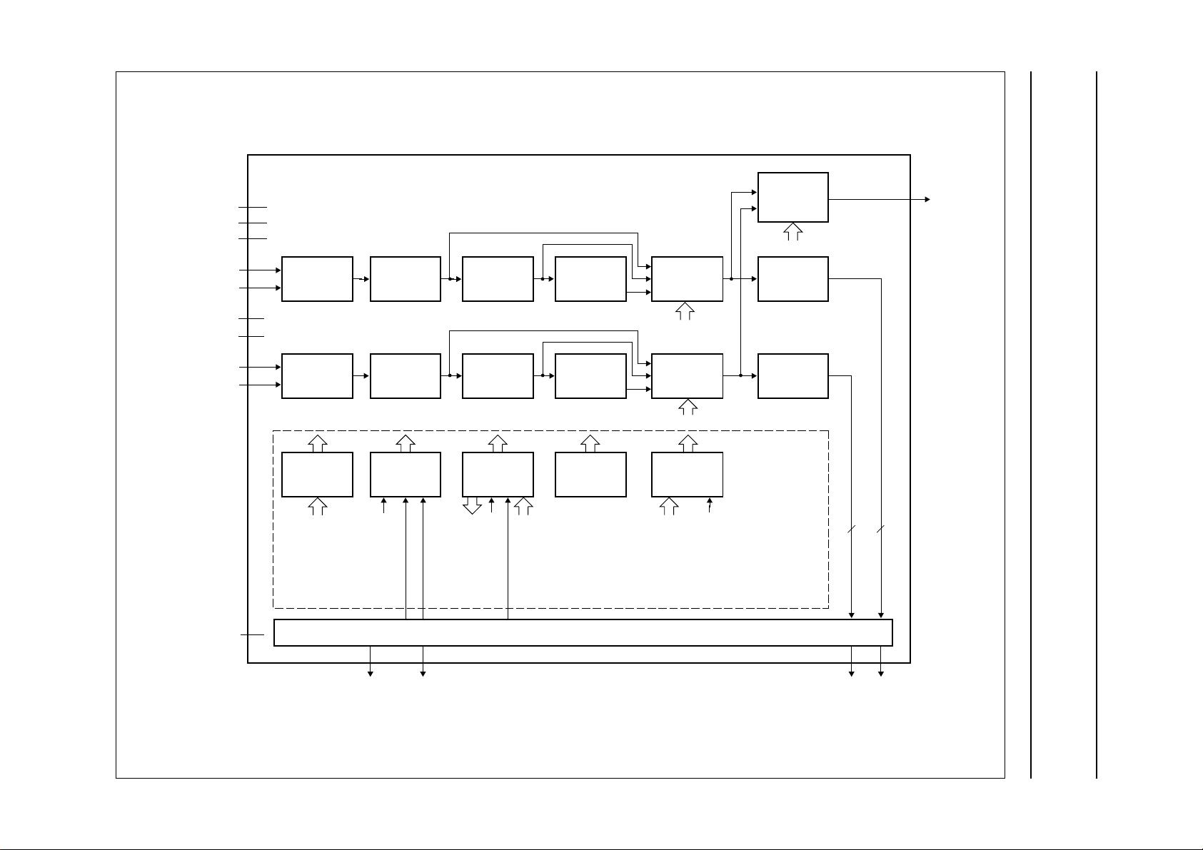
The digitized PAL, SECAM or NTSC signals AD1 (7 to 0)
and AD2 (7 to 0) are connected directly to the VPO-bus
via I
2
C-bus bit VIPB = 1 and MODE = 4, 5, 6 or 7.
AD1 (7 to 0) → VPO (15 to 8) and
AD2 (7 to 0) → VPO (7 to 0).
The selection of the analog input channels is controlled via
I
2
C-bus subaddress 02 MODE select.
The upsampled 8-bit offset binary CVBS signal (VBI-data
bypass) is multiplexed under control of the I
2
C-bus to the
digital VPO-bus (see Fig.8).
8.8 Reference signals HREF, VREF and CREF
• HREF: The positive slope of the HREF output signal
indicates the beginning of a new active video line.
The high period is 720 luminance samples long and is
also present during the vertical blanking.
The description of timing and position from HREF is
illustrated in Figs 15, 16, 21 and 23.
• VREF: The VREF output delivers a vertical reference
signal or an inverse composite blank signal controlled
via the I
2
C-bus [subaddress 11, inverse composite
blank (COMPO)]. Furthermore four different modes of
vertical reference signals are selectable via the I
2
C-bus
[subaddress 13, vertical reference output control
(VCTR1 and VCTR0)]. The description of VREF timing
and position is illustrated in Figs 15, 16, 24 and 25.
• CREF: The CREF output delivers a clock/pixel qualifier
signal for external interfaces to synchronize to the
VPO-bus data stream.
Four different modes for the clock qualifier signal are
selectable via the I
2
C-bus [subaddress 13, clock
reference output control (CCTR1 and CCTR0)].
The description of CREF timing and position is
illustrated in Figs 16, 18, 20 and 21.
8.9 Synchronization
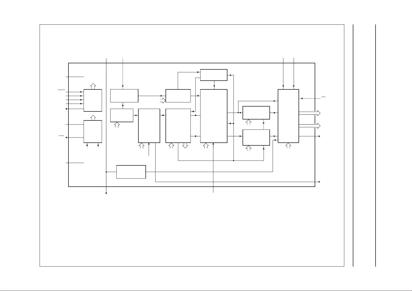
The prefiltered luminance signal is fed to the
synchronization stage. Its bandwidth is reduced to 1 MHz
in a low-pass filter. The sync pulses are sliced and fed to
the phase detectors where they are compared with the
sub-divided clock frequency. The resulting output signal is
applied to the loop filter to accumulate all phase
deviations. Internal signals (e. g. HCL and HSY) are
generated in accordance with analog front-end
requirements. The output signals HS, VS, and PLIN are
locked to the timing reference, guaranteed between the
input signal and the HREF signal, as further improvements
to the circuit may change the total processing delay. It is
therefore not recommended to use them for applications
which require absolute timing accuracy on the input
signals. The loop filter signal drives an oscillator to
generate the line frequency control signal LFCO
(see Fig.7).
8.10 Clock generation circuit
The internal CGC generates all clock signals required for
the video input processor. The internal signal LFCO is a
digital-to-analog converted signal provided by the
horizontal PLL. It is the multiple of the line frequency
Internally the LFCO signal is multiplied by a factor of 2 or 4
in the PLL circuit (including phase detector, loop filtering,
VCO and frequency divider) to obtain the LLC and LLC2
output clock signals. The rectangular output clocks have
a 50% duty factor (see Fig.26).
6.75MHz
429
432
----------
f
H
×=


