628 IEEE JOURNAL ON EMERGING AND SELECTED TOPICS IN CIRCUITS AND SYSTEMS, VOL. 2, NO. 3, SEPT EMBER 201
2
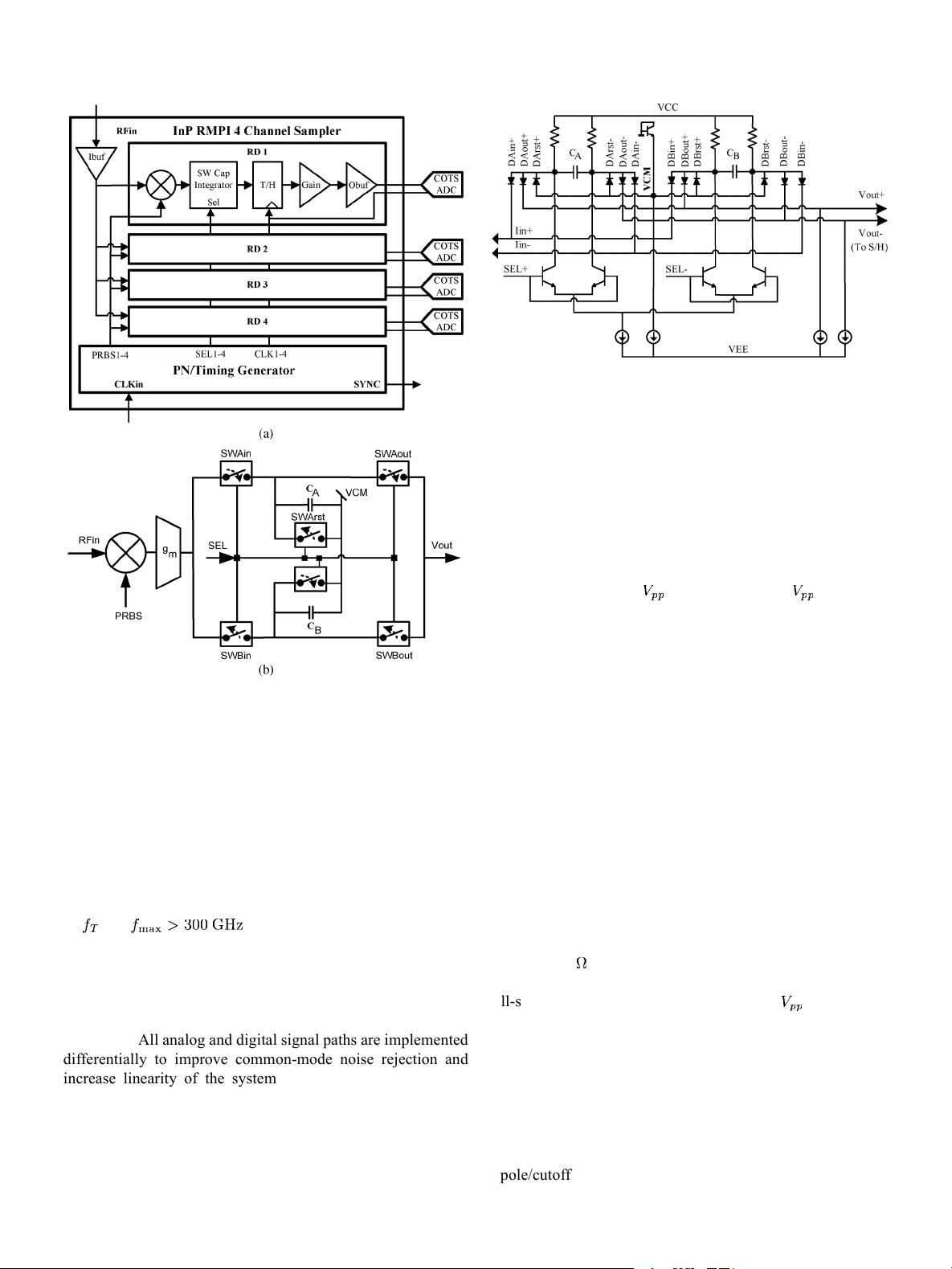
Fig. 1. (a) Simplified block diagram of 4-channel RMPI. The analog-signal
path of each RD channel is identical, however the tim ing signals they receive
in operation ar e d ifferent. ( b) Functional diagr am of the mixer and integrator
circuits. (a) System block diagram. (b) RD channel block diagram.
III. HA RDWARE IMPLEMENTATION DESCRIPTION
A. Architecture and Operation
The RMPI presented in this work was realized with the
proprietary Northrop Grumman (NG) 450 nm InP H BT bipolar
process [26]. The process features a four-layer metal stack with
an
and . Fig. 1 (a) shows the block diagram
of the integrated circuit (IC) containing the inp ut b uffer driving
the common node of the four RD channels and the tim ing gen-
erator. The timing generator is responsible for generating the
pseudo-random bit sequences (PRBS) and the clocking wave-
forms t o coordinate the track-and-hold (T/H) and integration
operations. All analog and digital signal paths are implem ented
differentially to improve common-mode n oise rejection and
increase linearity of the system. The analog path up to the
integrator was designed f or a 2.5 GHz bandwidth. The ensuin g
integration reduces the bandwidth containing significant energy
content. The circuit s fo llowing the integrator ar e designed to
meet the settling requ irements of the reduced bandwidth. A
5 GHz master clock reference (CLKin) is used to toggle the
PRBS generators and is chosen to be the N yquist-rate of the
input band wid th [12], [17]. T he T/H o perates at 1/52 the master
Fig. 2. Simplified schematic of interleaved s witched capacitor integra to r. The
diodes act as switches to configure capacitors for integratio n or reset it based
on the level of the control sign a l (SEL). W h e n SEL is asserted, integrator A is
resetting and integrator B is in teg rating. When SEL is d e-asser ted, integrator B
is resettin g and integrator A is integ rating.
clock frequency (96.154 MHz). A switched-capacitor inter-
leaving integrator [27] is used so that one capacitor can be reset
while the second integrates the mixer output. Finally, an ou tpu t
buffer is designed t o drive the ADC with the correct swing an d
common-mode voltage. The chip was designed for a full-scale
input amplitude of 0.5
differential and 1 differential
output. In opera tio n, the RMPI circuit tak e s the analog input
signal, buffers it, and distributes the buffered signal to each
of the four channels. In each channel, the signal is multiplied
by one of four orthogonal PR BS—each of which is a 3276 bit
long Gold code [28]. T he resulting prod uct is integrated by one
of two sets of interleaved capacitors for exactly one frame (52
CLKin cy c les). At the end of the integration period the signal is
sampled and then held for 26 CLKin cycles to allow the external
ADC t o digitize t he signal for postpr ocessing . Immediately
after the signal is sampled, the capacitor begins discharging
and the second capacitor begins integrating the next frame [see
Fig. 1(b)]. The interleaved integration capacitors are used to
avoid missing frames due to the reset operation. Additionally,
the sam pling instants for each channel are staggered to create
more diversity in the windowed integrations obtained.
B. Analog Signa l Path
The input buffer is a differential pair with emitter degener-
ation and 50
termination at each single-ended input. It has
a gain of 3 dB, a 2.5 GHz bandwidth, 70 dB SFDR, and a
full-scale d ifferential input amplitu de of 0.5
. T he random
modulation is perfo rm ed by a standard differential Gilbert
mixer with the PRBS generator driving the top two pairs and
the analog input driv ing the bottom differential pair. Emitter
degeneration is used on the bottom differential pair to im prove
linearity. To reduce n oise, the m ixer was designed to have
about 20 dB gain to compensate for the attenuation from the in-
tegrator. T he output of the mixer is integrated using interleaved
switched capacitors as shown in Fig. 1(b) and Fig. 2 and has
a pole/cutoff frequency located at 12.5 MHz. Diode switches
route the mixer output current to the integration capacito r, read
out the capacitor voltage, and reset it to zero at the end of a


