TI LMK61E0M:高性能集成振荡器,具备低抖动与I2C配置功能
需积分: 5 13 浏览量
更新于2024-06-28
4
收藏 1.14MB PDF 举报
TI-LMK61E0M是一款高性能、超低抖动的集成振荡器,专为各种高精度和低噪声应用设计。该产品具备以下主要特点:
1. **卓越性能**:
- LMK61E0M以其典型的500 femtoseconds (fs) RMS噪声水平,在输出频率高于50MHz时,提供了极低的抖动特性。
- 该振荡器最高支持200MHz的3.3V LVCMOS输出,满足高速信号处理的需求。
2. **系统级特性**:
- 提供宽广的频率容差范围,达到±25 parts per million (ppm),确保了稳定且准确的频率输出。
- 内置EEPROM允许用户进行自定义启动设置,增加了灵活性和定制化能力。
3. **接口与控制**:
- 支持快速模式I2C通信,频率可达1000kHz,便于设备控制和配置。
- 设计适用于3.3伏电源工作环境,兼容工业级温度范围(-40°C 至 +85°C)。
4. **紧凑封装**:
- 采用7毫米×5毫米的8引脚封装,占用空间小,适合小型化设计。
5. **广泛的应用领域**:
- 作为高质量晶体振荡器、SAW振荡器或芯片振荡器的替代选择,适用于高精度电子设备,如开关、路由器、网卡、基带单元(BBU)、服务器、存储设备、SAN等。
- 在测试和测量设备,特别是医疗成像技术中,由于其低抖动特性,非常适合对时间精确度要求高的场景。
- 也适用于FPGA和处理器之间的连接,以及xDSL等通信技术。
6. **重要注意事项**:
- 产品末尾的"IMPORTANT NOTICE"部分包含了关于产品可用性、保修、安全关键应用使用、知识产权声明以及使用限制的免责声明,请在使用前仔细阅读。
综上,LMK61E0M是一款高性价比的振荡器解决方案,其设计考虑到了性能、可靠性和易用性,适用于多种现代电子设备中的频率基准需求。
Output
Control
Power Conditioning
VDD
od
EEPROMRegisters
od
SCL
SDA
od = open-drain
PLL
VCO: 4.6 GHz ~ 5.6 GHz
¥
10 nF
Device
Control
3
ADD
Integrated
Oscillator
XO
N Div
™ûfractional
3 = tri-state
Integer Div
GND
OE
R Div
/1, /4
Doubler
x1, x2
OUT0
OUT1
Copyright © 2017, Texas Instruments Incorporated
9
LMK61E0M
www.ti.com.cn
ZHCSG16A –JANUARY 2017–REVISED MAY 2017
Copyright © 2017, Texas Instruments Incorporated
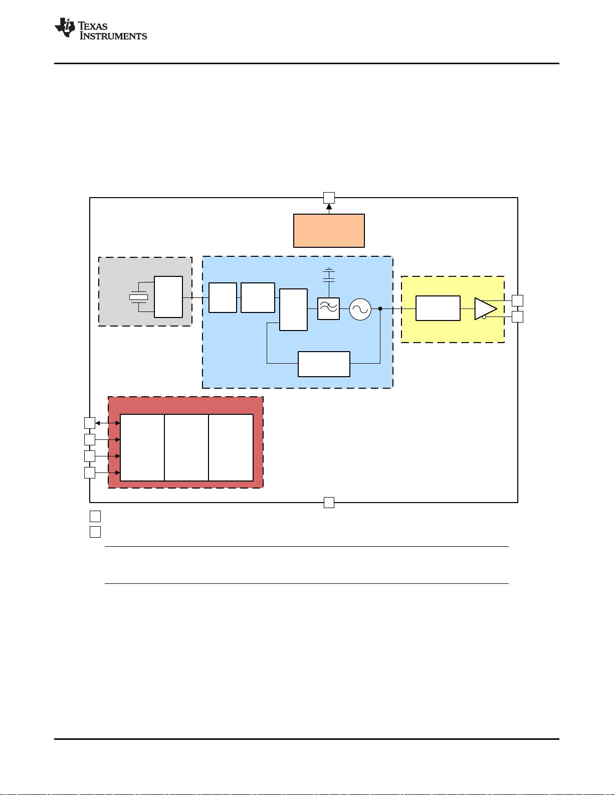
8 Detailed Description
8.1 Overview
The LMK61E0 is a programmable oscillator family that generates commonly used reference clocks. LMK61E0M
supports 3.3-V LVCMOS outputs with less than 1000-fs RMS max jitter in integer PLL and fractional PLL modes.
8.2 Functional Block Diagram
NOTE
Control blocks are compatible with 1.8-V, 2.5-V, and 3.3-V I/O voltage levels.
8.3 Feature Description
8.3.1 Device Block-Level Description
The LMK61E0 is an integrated oscillator that includes a 50-MHz crystal and a fractional PLL with integrated VCO
that supports a frequency range of 4.6 GHz to 5.6 GHz. The PLL block consists of a phase frequency detector
(PFD), charge pump, integrated passive loop filter, a feedback divider that can support both integer and fractional
values and a delta-sigma engine for noise suppression in fractional PLL mode. Completing the device is the
combination of an integer output divider and an LVCMOS output buffer. The PLL is powered by on-chip low
dropout (LDO) linear voltage regulators and the regulated supply network is partitioned such that the sensitive
analog supplies are running from separate LDOs than the digital supplies which use their own LDO. The LDOs
provide isolation to the PLL from any noise in the external power supply rail. The device supports fine and coarse
frequency margining by changing the settings of the integrated oscillator and the output divider respectively.
剩余47页未读,继续阅读
点击了解资源详情
点击了解资源详情
点击了解资源详情
2022-11-30 上传
2022-11-30 上传
2022-11-30 上传
2022-11-30 上传
2022-11-30 上传
2022-11-30 上传

不觉明了
- 粉丝: 4502
- 资源: 5759
 我的内容管理
展开
我的内容管理
展开


最新资源
- MATLAB新功能:Multi-frame ViewRGB制作彩色图阴影
- XKCD Substitutions 3-crx插件:创新的网页文字替换工具
- Python实现8位等离子效果开源项目plasma.py解读
- 维护商店移动应用:基于PhoneGap的移动API应用
- Laravel-Admin的Redis Manager扩展使用教程
- Jekyll代理主题使用指南及文件结构解析
- cPanel中PHP多版本插件的安装与配置指南
- 深入探讨React和Typescript在Alias kopio游戏中的应用
- node.js OSC服务器实现:Gibber消息转换技术解析
- 体验最新升级版的mdbootstrap pro 6.1.0组件库
- 超市盘点过机系统实现与delphi应用
- Boogle: 探索 Python 编程的 Boggle 仿制品
- C++实现的Physics2D简易2D物理模拟
- 傅里叶级数在分数阶微分积分计算中的应用与实现
- Windows Phone与PhoneGap应用隔离存储文件访问方法
- iso8601-interval-recurrence:掌握ISO8601日期范围与重复间隔检查
