7
LP8867C-Q1
,
LP8869C-Q1
www.ti.com.cn
ZHCSK37 –AUGUST 2019
Copyright © 2019, Texas Instruments Incorporated
(1) Output Current Accuracy is the difference between the actual value of the output current and programmed value of this current.
Matching is the maximum difference from the average. For the constant current sinks on the part (OUTx), the following are determined:
the maximum output current (MAX), the minimum output current (MIN), and the average output current of all outputs (AVG). Matching
number is calculated: (MAX-MIN)/AVG. The typical specification provided is the most likely norm of the matching figure for all parts. LED
current sinks were characterized with 1-V headroom voltage. Note that some manufacturers have different definitions in use.
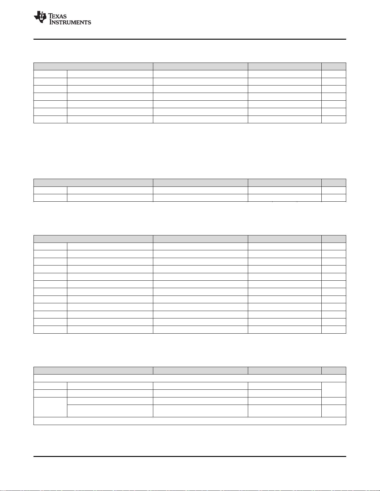
7.8 Current Sinks Electrical Characteristics
Limits apply over the full operation temperature range −40°C ≤ T
A
≤ +125°C , unless otherwise speicified, V
IN
= 12V.
PARAMETER TEST CONDITIONS MIN TYP MAX UNIT
I
LEAKAGE
Leakage current Outputs OUT1 to OUT4 , V
OUTx
= 45 V, EN = L 0.1 5 µA
I
MAX
Maximum current OUT1, OUT2, OUT3, OUT4, R
ISET
= 20 kΩ 120 mA
I
OUT
Output current accuracy I
OUT
= 100 mA −5% 5%
I
MATCH
Output current matching
(1)
I
OUT
= 100 mA, PWM duty =100% 1% 5%
V
LOW_COMP
Low comparator threshold 0.9 V
V
MID_COMP
Mid comparator threshold 1.9 V
V
HIGH_COMP
High comparator threshold 5.6 6 7 V
(1) This specification is not ensured by ATE.
7.9 PWM Brightness Control Electrical Characteristics
Limits apply over the full operation temperature range −40°C ≤ T
A
≤ +125°C , unless otherwise speicified, V
IN
= 12V.
PARAMETER TEST CONDITIONS MIN TYP MAX UNIT
ƒ
PWM
PWM input frequency 100 20 000 Hz
t
ON/OFF
Minimum on/off time
(1)
0.5 µs
(1) This specification is not ensured by ATE.
7.10 Boost and SEPIC Converter Characteristics
Limits apply over the full operation temperature range −40°C ≤ T
A
≤ +125°C , unless otherwise speicified, V
IN
= 12V.
PARAMETER TEST CONDITIONS MIN TYP MAX UNIT
V
IN
Input voltage 4.5 40 V
V
OUT
Output voltage 6 45
ƒ
SW_MIN
Minimum switching frequency Defined by R
FSET
resistor 300 kHz
ƒ
SW_MAX
Maximum switching frequency Defined by R
FSET
resistor 2 200 kHz
t
OFF
Minimum switch OFF time
(1)
ƒ
SW
≥ 1.15 MHz 55 ns
I
SW_MAX
SW current limit first triggerred 3.3 3.7 4.1 A
t
SW_MAX
SW current limit first triggerred period 1.6 s
I
SW_LIM
SW current limit 3 3.35 3.7 A
R
DSON
FET R
DSON
240 400 mΩ
f
SYNC
External SYNC frequency 300 2 200 kHz
t
SYNC_ON
External SYNC on time
(1)
150 ns
t
SYNC_OFF
External SYNC off time
(1)
150 ns
7.11 Logic Interface Characteristics
Limits apply over the full operation temperature range −40°C ≤ T
A
≤ +125°C , unless otherwise speicified, V
IN
= 12V.
PARAMETER TEST CONDITIONS MIN TYP MAX UNIT
LOGIC INPUT VDDIO/EN
V
IL
Input low level 0.4
V
V
IH
Input high level 1.65
I
EN
Input DC current −1 5 30 µA
Input transient current during VDDIO/EN
powering up
1.2 mA
LOGIC INPUT SYNC, PWM


