Design and fabrication of wavelength tunable AWGs
based on the thermo-optic effect
Pei Yuan (袁 配)
1,2
, Yue Wang (王玥)
1,
*, Yuanda Wu (吴远大)
1,2
,
Junming An (安俊明)
1,2
, and Xiongwei Hu (胡雄伟)
1
1
State Key Laboratory on Integrated Optoelectronics, Institute of Semiconductors, Chinese Academy of Science,
Beijing 100083, China
2
College of Materials Science and Opto-Electronic Technology, University of Chinese Academy of Sciences,
Beijing 100083, China
*Corresponding authors: wy1022@semi.ac.cn
Received September 29, 2017; accepted October 13, 2017; posted online November 9, 2017
In this Letter, a 16 channel 200 GHz wavelength tunable arrayed waveguide grating (AWG) is designed and
fabricated based on the silicon on insulator platform. Considering that the performance of the AWG, such as
central wavelength and crosstalk, is sensitive to the dimension variation of waveguides, the error analysis of the
AWG with width fluctuations is worked out using the transfer function method. A heater is designed to realize
the wavelength tunability of the AWG based on the thermo-optic effect of silicon. The measured results show
that the insertion loss of the AWG is about 6 dB, and the crosstalk is 7.5 dB. The wavelength tunability of 1.1 nm
is achieved at 276 mW power consumption, and more wavelength shifts will gain at larger power consumption.
OCIS codes: 060.1810, 060.4230, 230.7390, 230.7408.
doi: 10.3788/COL201816.010601.
Silicon photonics
[1– 3]
, as a low cost integration platform
for datacom and telecom applications, has been drawing
a lot of attention nowadays. Silicon on insulator (SOI)
is an ideal material for separating passive or active
devices
[4– 9]
and their integration
[10–13]
because of its trans-
parent optical property over the communication band.
Besides, the mature CMOS technology can be directly
applied to the integration of silicon photonics devices,
which can lower their production cost greatly. With
high-index contrast, the bending radius of SOI bent
waveguides can be fabricated in a very small size with
low loss, so the devices bas ed on SOI may have a
compact and small footprint. However, the high-index
contrast of SOI material will induce some issues; for
example, the properties of SOI devices are sensitive to
the dimensional variation of their waveguides, thus,
resulting in small fabrication tolerance and difficulty in
fabrication. The arrayed waveguide grating (AWG)
[14–18]
is an interference device used in the wavelength division
multiplexing (WDM) system, which is sensitive to the
change of phase. When the regular phase is damaged,
the transmission spectrum of the AWG will get worse.
More concretely, when the fabrication dimension of the
waveguides deviate from their designed value, the regular
phase will change, then the peak wavelength of the AWG
will drift, and the crosstalk will be poor as well. Therefore,
compensation for the wavelength shift of the AWG is
necessary. There are many reports about wavelength tun-
able AWGs based on silica
[19]
,InP
[20]
, and polymer
[21]
,but
there are only a few on wavelength tunable AWG based
on SOI
[22]
.
In this Letter, the simulation and the error analysis of
AWGs with width fluctuations are worked out to analyze
the influence of waveguide width on the crosstalk of the
AWG. Then, the AWG with heaters for realizing channel
tunability based on the thermo-optic (TO) effect of silicon
is designed and fabricated.
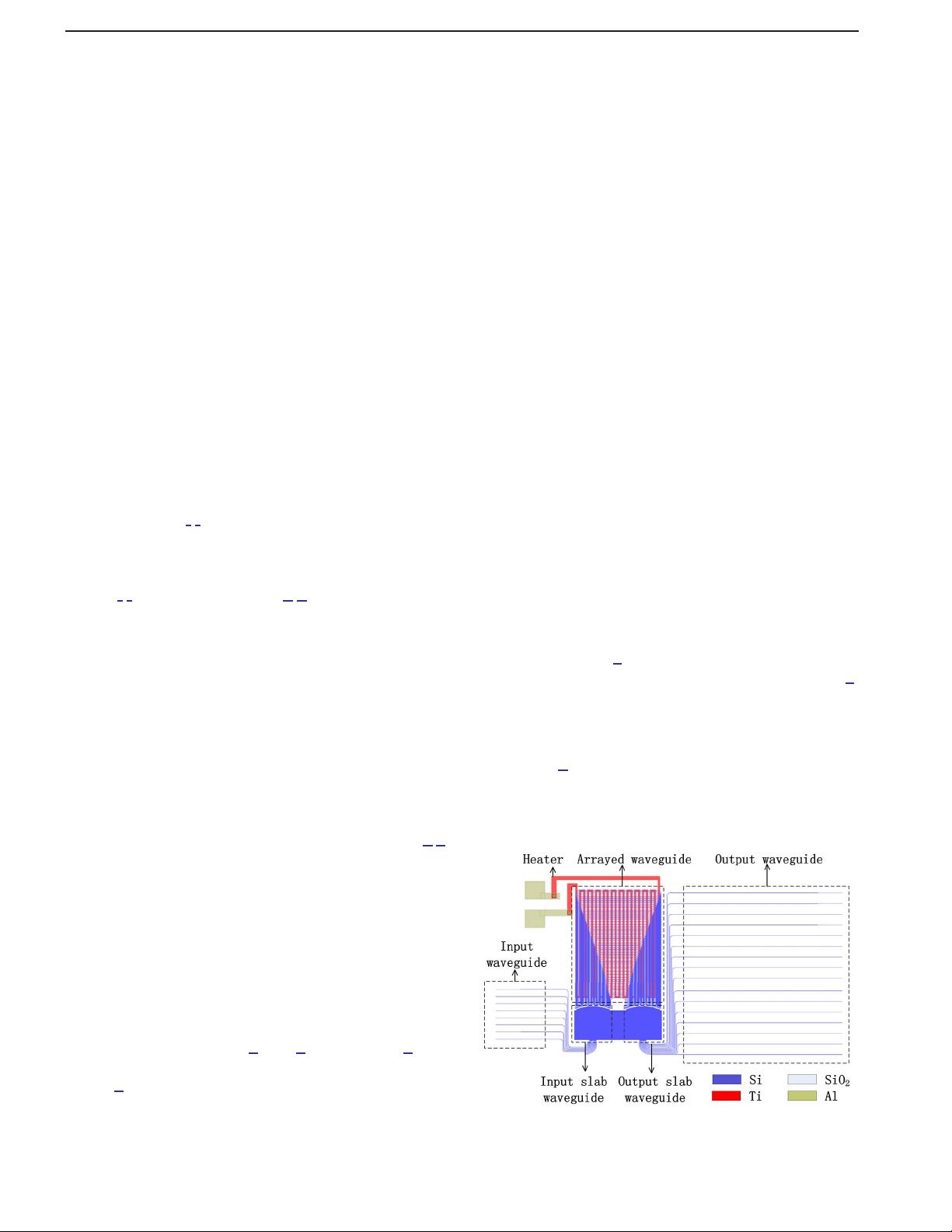
A typical AWG consists of input/output waveguides,
input/output slab waveguides, and arrayed waveguides;
heaters are designed to realize the tunable wavelength,
as is shown in Fig.
1. The design parameters of the 16
channel 200 GHz AWG in this Letter are listed in Table
1.
As the performance, such as peak wavelength and cross-
talk of the AWG, is sensitive to the fabricated dimension,
the simulation and the error analysis of AWGs with width
fluctuations are worked out by adopting the transfer func-
tion method
[23]
. Without considering the transmission loss,
the transfe r function with the width fluctuations can be
depicted as
Fig. 1. (Color online) Schematic diagram of a typical AWG.
COL 16(1), 010601(2018) CHINESE OPTICS LETTERS January 10, 2018
1671-7694/2018/010601(5) 010601-1 © 2018 Chinese Optics Letters


