3
DDR3 Demo for the
Lattice Semiconductor LatticeECP3 Versa Evaluation Board
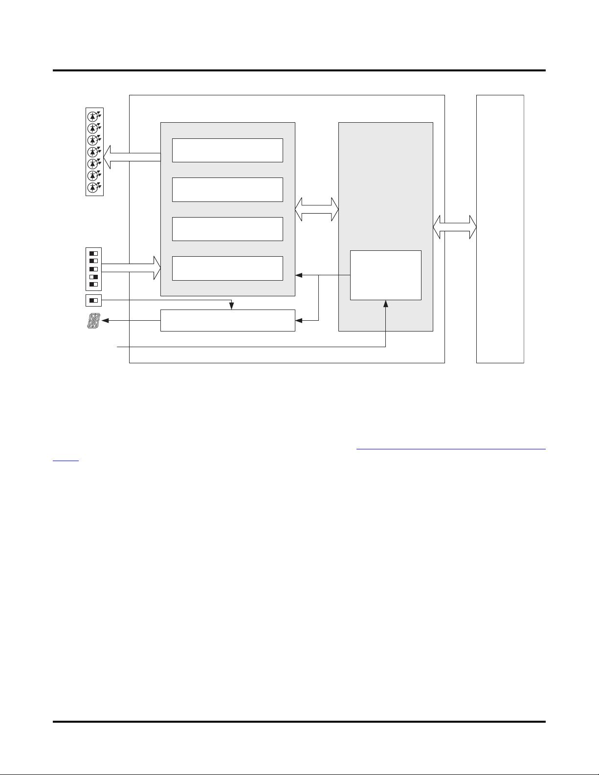
Figure 1. DDR3 Demo Design Block Diagram
CSM
14-Segment LED Driver
Command Generator
(State Machine)
Address Generator
Write Data Generator
Read Data Validator
LatticeECP3-35EA
DDR_ulogic
DDR3 Memory
Controller
Local User
Interface
100MHz DDR3
Clock Input
200MHz
SCLK
On-Board
DDR3
SDRAM
DDR3
Inteface
6-Bit DIP Switch
7 Output LEDs
DDR3 SDRAM Controller IP Core
The IP core used to generate the DDR3 controller core is the DDR3 SDRAM Controller IP core, version 1.2. The
user must install version 1.2 before generating the IP core and running the demo. The core generated with this IP
core interfaces directly with the external, on-board DDR3 SDRAM and performs control operations. The demo has
been designed to support a DDR3 data bus width of 16 bits since the DDR3 memory module installed in the
LatticeECP3 Versa Evaluation Board is 16 bits wide. See EB62, the
LatticeECP3 Versa Development Kit User’s
Guide for further information on the DDR3 SDRAM module used in this demo. Once a DDR3 core is generated with
a supported data width, the whole demo design can be simulated and implemented without modifying the code. A
DDR3
IP core configuration file (ddr3core.lpc) is provided in the demo package. This configuration file should be
used to make changes to the core and/or regenerate the core. In the Linux platform, the DDR3 SDRAM Controller
IP core should be downloaded, uncompressed and placed in the folder diamond/1.2/module. The DDR3 SDRAM
Controller IP core will appear in the IP core tree.
User Logic
The user logic implemented in the DDR3 demo design provides the following functions:
• State machine programs the mode registers and controls DDR3 read and write operations
• Address generation
• Write data generation
• Read data validation
• Control and observation
Demo Control State Machine
The state machine controls the demo using the user control input through a 6-bit DIP switch. Once the Lat-
t
iceECP3 device is programmed or a system reset is applied by pressing the GSR button, the state machine pro-
grams all DDR3 mode registers (MR0~MR3) based on the user test
configuration (DIP switch setting). Then, it gen-


