NXP Semiconductors
FXLS8962AF
3-Axis Low-g Accelerometer
FXLS8962AF All information provided in this document is subject to legal disclaimers. © NXP B.V. 2019. All rights reserved.
Product data sheet Rev. 5.3 — 10 December 2019
18 / 99
10.1.1 General I
2
C operation
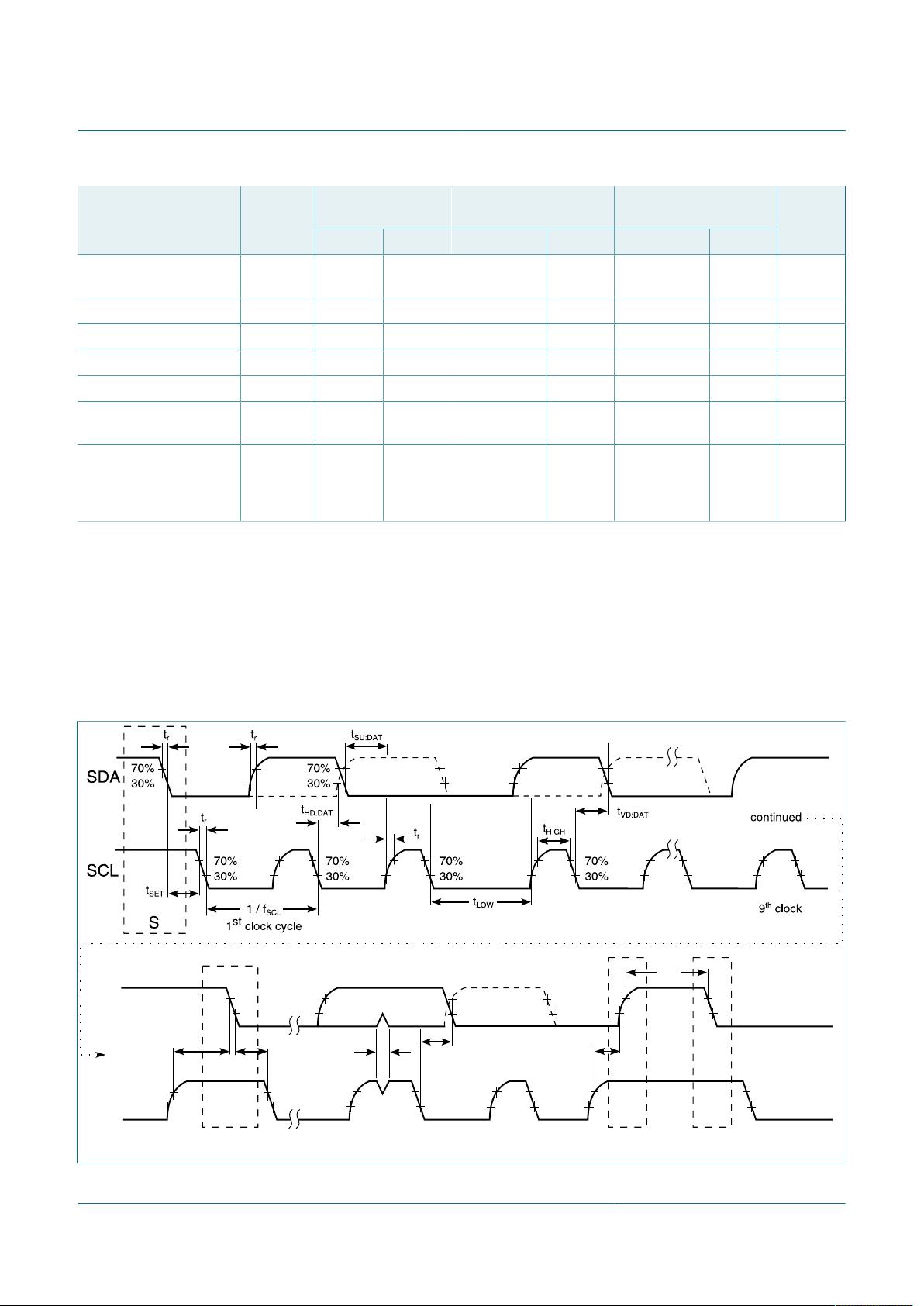
There are two signals associated with the I
2
C-bus: the Serial Clock Line (SCL) and the
Serial Data line (SDA). SDA is a bidirectional signal used for sending and receiving the
data to/from the interface. External pull-up resistors connected to V
DD
are required for
SDA and SCL. When the I
2
C-bus is free, SCL and SDA are high.
The maximum practical operating frequency for I
2
C in a given system implementation
depends on several factors including the pull-up resistor and voltage values and total bus
capacitance (PCB trace + parasitic device capacitance(s)).
A transaction on the bus is started by the master through a start condition (ST) signal,
which is defined as a HIGH-to-LOW transition on SDA line while the SCL line is held
HIGH. After the ST signal has been transmitted by the master, the bus is considered
busy. The next byte of data transmitted contains the slave address in the first seven
bits, and the eighth bit, the read/write bit, indicates whether the master is receiving data
from the slave or transmitting data to the slave. When an address is sent, each device in
the system compares the first seven bits after the ST condition with its own address. If
they match, the device considers itself addressed by the master. The ninth clock pulse,
following the slave address byte (and each subsequent byte) is the acknowledge (ACK).
The transmitter must release the SDA line during the ACK period. The receiver must
then pull the data line low so that it remains stable low during the high period of the
acknowledge clock period.
The number of bytes per transfer is unlimited. If a receiver can't receive another complete
byte of data until it has performed some other function, it can hold the SCL line low to
force the transmitter into a wait state. Data transfer only continues when the receiver
is ready for another byte and releases the clock line. This delay action is called clock
stretching. Not all master devices support clock stretching. This device implements clock
stretching—the SCL line may be stretched (pulled low) for up to 1 µs when needed
during a read operation. Clock stretching, when applied, will occur after the ACK is
issued by the I
2
C bus master.
A LOW-to-HIGH transition on the SDA line while the SCL line is high is defined as a stop
condition (SP) signal. A write or burst write is always terminated by the master issuing
the SP signal. A master should properly terminate a read by not acknowledging a byte at
the appropriate time in the protocol, followed by the SP signal. A master may also issue a
repeated start signal (SR) during a transfer.
10.1.2 I
2
C read/write operations
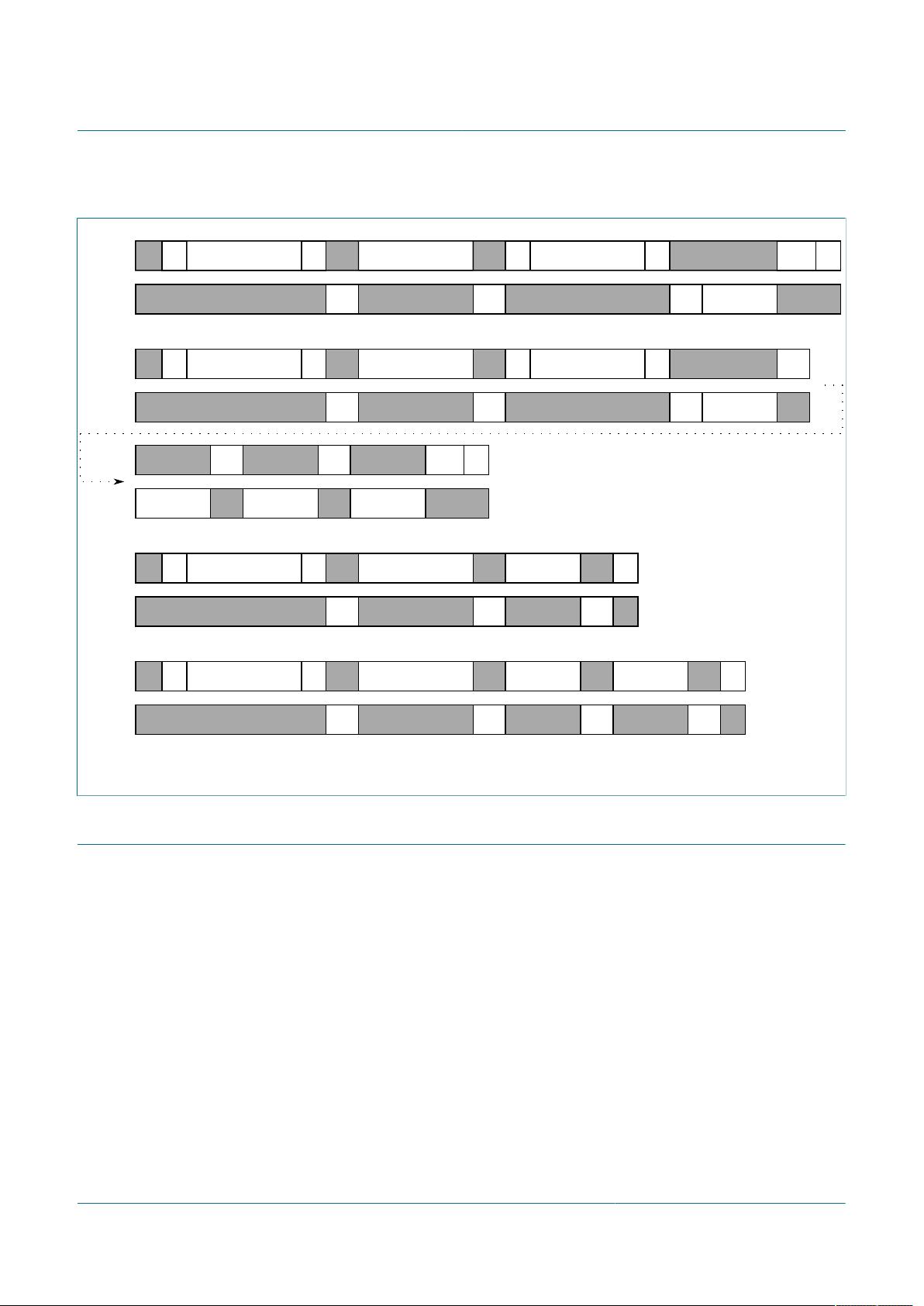
10.1.2.1 Single byte read
The master transmits a start condition (ST) to FXLS8962AF, followed by the slave
address, with the R/W bit set to '0' for a write, and the FXLS8962AF sends an
acknowledgement. Then the master transmits the address of the register to read and
the FXLS8962AF sends an acknowledgement. The master transmits a repeated start
condition (SR), followed by the slave address with the R/W bit set to '1' for a read from
the previously selected register. The FXLS8962AF then acknowledges and transmits
the data from the requested register. The master does not acknowledge (NAK) the
transmitted data and then transmits a stop condition to end the data transfer.
10.1.2.2 Multiple byte read
When performing a multi-byte or burst read, FXLS8962AF automatically increments the
register read address pointer after a read command is received. Therefore, after following


