没有合适的资源?快使用搜索试试~ 我知道了~
首页英文版电子设备与电路理论——半导体二极管深入解析
英文版电子设备与电路理论——半导体二极管深入解析
需积分: 50 8 下载量 164 浏览量
更新于2024-07-22
收藏 21.08MB PDF 举报
"这是一本全面的英文模拟电子设备与电路理论教材,由Robert Boylestad和Louis Nashelsky合著,由Prentice Hall出版社出版。本书内容涵盖半导体二极管的基本概念、应用以及相关电路分析。"
在本书中,作者深入浅出地介绍了模拟电子技术的基础知识,特别是关于半导体二极管的方方面面。第1章"半导体二极管"首先从介绍入手,讲解了理想二极管的概念,并讨论了半导体材料的性质,如能量级和杂质半导体(n型和p型)。接着,书中详细阐述了半导体二极管的工作原理,包括电阻特性、等效电路、规格表、势垒和扩散电容、反向恢复时间、二极管符号以及二极管的测试方法。此外,还特别提到了稳压二极管(Zener二极管)和发光二极管(LEDs)的应用,以及二极管阵列和集成电路。
第2章"二极管应用"则将焦点转向二极管在实际电路中的使用。这部分内容涵盖了负载线分析、二极管近似模型、带有直流输入的串联二极管配置、并联和串并联配置、逻辑门(AND/OR门)、正弦波输入下的半波整流、全波整流、钳位电路以及电压钳位器。此外,Zener二极管在电压调节中的作用也得到了详细阐述。
通过这本书,读者不仅可以掌握半导体二极管的基础知识,还能了解到如何在各种电路设计中有效地运用这些知识。无论是对于初学者还是有一定基础的学习者,这本书都提供了丰富的学习材料,有助于提升对模拟电子电路的理解和实践能力。对于想要深入理解和应用模电知识的人来说,这无疑是一本非常有价值的参考资料。

5
p n
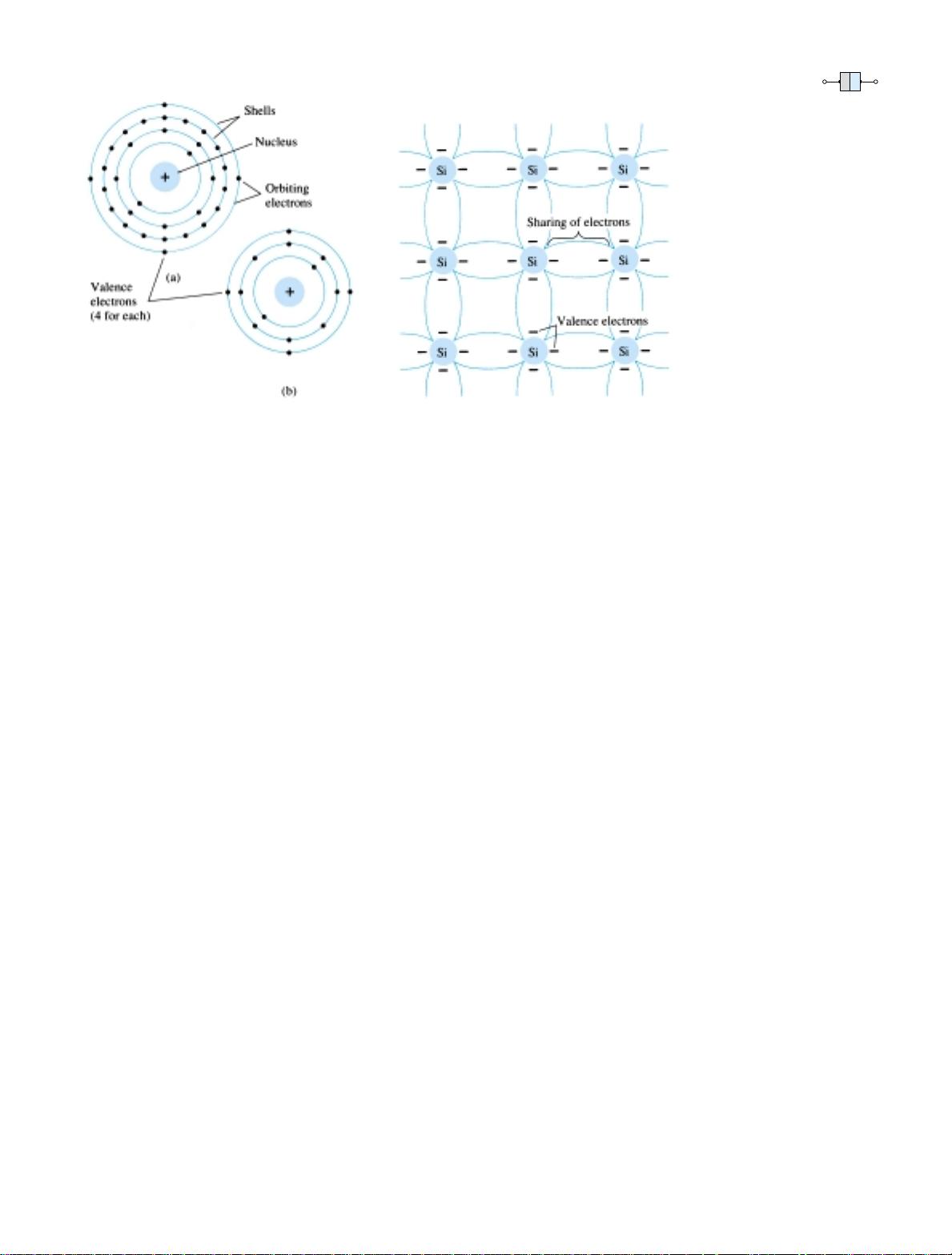
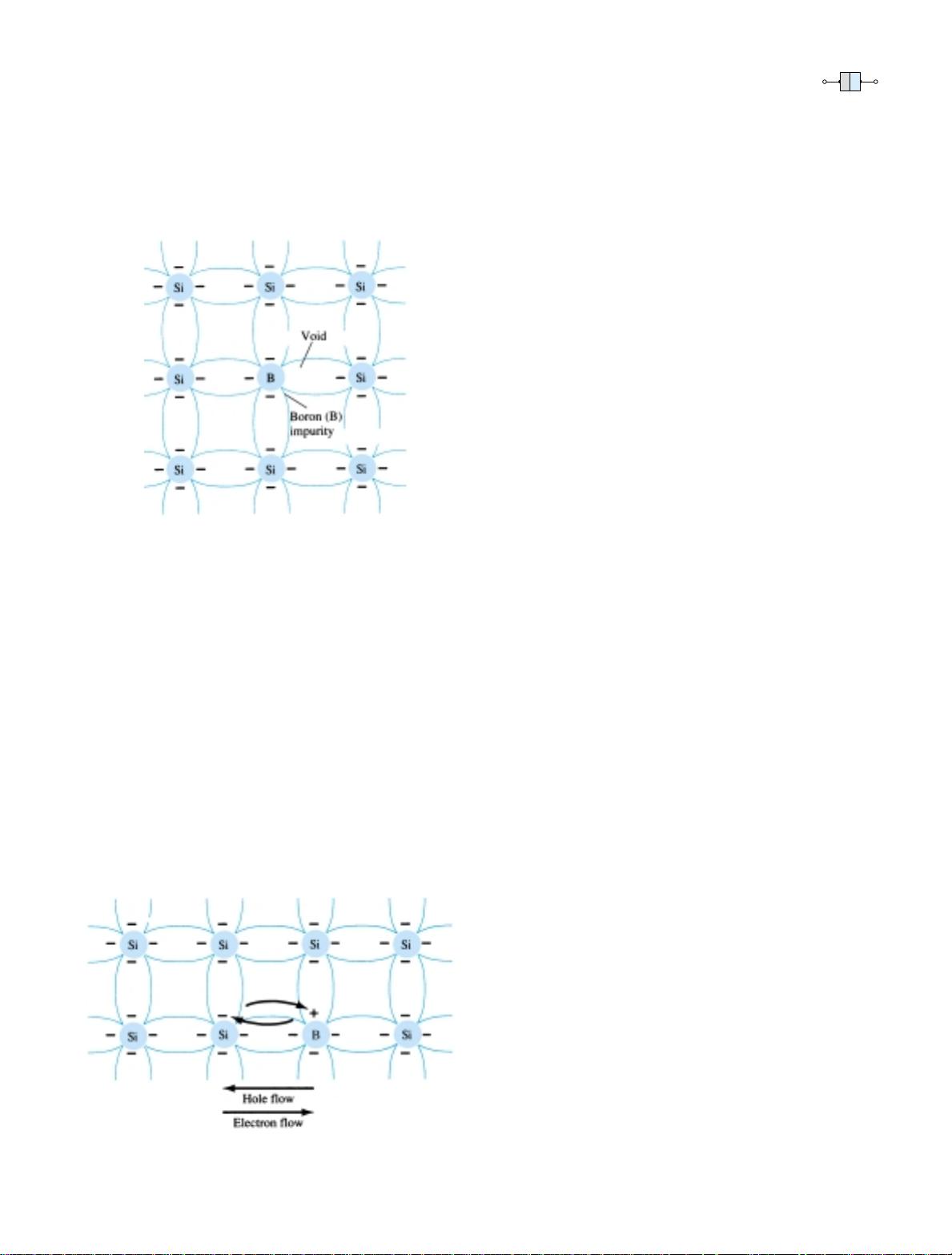
Although the covalent bond will result in a stronger bond between the valence
electrons and their parent atom, it is still possible for the valence electrons to absorb
sufficient kinetic energy from natural causes to break the covalent bond and assume
the “free” state. The term free reveals that their motion is quite sensitive to applied
electric fields such as established by voltage sources or any difference in potential.
These natural causes include effects such as light energy in the form of photons and
thermal energy from the surrounding medium. At room temperature there are approx-
imately 1.5 10
10
free carriers in a cubic centimeter of intrinsic silicon material.
Intrinsic materials are those semiconductors that have been carefully refined
to reduce the impurities to a very low level—essentially as pure as can be
made available through modern technology.
The free electrons in the material due only to natural causes are referred to as
intrinsic carriers. At the same temperature, intrinsic germanium material will have
approximately 2.5 10
13
free carriers per cubic centimeter. The ratio of the num-
ber of carriers in germanium to that of silicon is greater than 10
3
and would indi-
cate that germanium is a better conductor at room temperature. This may be true,
but both are still considered poor conductors in the intrinsic state. Note in Table 1.1
that the resistivity also differs by a ratio of about 10001, with silicon having the
larger value. This should be the case, of course, since resistivity and conductivity are
inversely related.
An increase in temperature of a semiconductor can result in a substantial in-
crease in the number of free electrons in the material.
As the temperature rises from absolute zero (0 K), an increasing number of va-
lence electrons absorb sufficient thermal energy to break the covalent bond and con-
tribute to the number of free carriers as described above. This increased number of
carriers will increase the conductivity index and result in a lower resistance level.
Semiconductor materials such as Ge and Si that show a reduction in resis-
tance with increase in temperature are said to have a negative temperature
coefficient.
You will probably recall that the resistance of most conductors will increase with
temperature. This is due to the fact that the numbers of carriers in a conductor will
1.3 Semiconductor Materials
Figure 1.6 Atomic structure: (a) germanium;
(b) silicon.
Figure 1.7 Covalent bonding of the silicon
atom.

not increase significantly with temperature, but their vibration pattern about a rela-
tively fixed location will make it increasingly difficult for electrons to pass through.
An increase in temperature therefore results in an increased resistance level and a pos-
itive temperature coefficient.
1.4 ENERGY LEVELS
In the isolated atomic structure there are discrete (individual) energy levels associated
with each orbiting electron, as shown in Fig. 1.8a. Each material will, in fact, have
its own set of permissible energy levels for the electrons in its atomic structure.
The more distant the electron from the nucleus, the higher the energy state,
and any electron that has left its parent atom has a higher energy state than
any electron in the atomic structure.
6
Chapter 1 Semiconductor Diodes
p n
Figure 1.8 Energy levels: (a)
discrete levels in isolated atomic
structures; (b) conduction and
valence bands of an insulator,
semiconductor, and conductor.
Energy
Energy Energy
E > 5 eV
g
Valence band
Conduction band
Valence band
Conduction band
Conduction band
The bands
overlap
Electrons
"free" to
establish
conduction
Valence
electrons
bound to
the atomic
stucture
E = 1.1 eV (Si)
g
E = 0.67 eV (Ge)
g
E = 1.41 eV (GaAs)
g
Insulator Semiconductor
(b)
E
g
E
Valence band
Conductor
Energy gap
Energy gap
etc.
Valance Level (outermost shell)
Second Level (next inner shell)
Third Level (etc.)
Energy
Nucleus
(a)
Between the discrete energy levels are gaps in which no electrons in the isolated
atomic structure can appear. As the atoms of a material are brought closer together to
form the crystal lattice structure, there is an interaction between atoms that will re-
sult in the electrons in a particular orbit of one atom having slightly different energy
levels from electrons in the same orbit of an adjoining atom. The net result is an ex-
pansion of the discrete levels of possible energy states for the valence electrons to
that of bands as shown in Fig. 1.8b. Note that there are boundary levels and maxi-
mum energy states in which any electron in the atomic lattice can find itself, and there
remains a forbidden region between the valence band and the ionization level. Recall

that ionization is the mechanism whereby an electron can absorb sufficient energy to
break away from the atomic structure and enter the conduction band. You will note
that the energy associated with each electron is measured in electron volts (eV). The
unit of measure is appropriate, since
W QV eV (1.2)
as derived from the defining equation for voltage V W/Q. The charge Q is the charge
associated with a single electron.
Substituting the charge of an electron and a potential difference of 1 volt into Eq.
(1.2) will result in an energy level referred to as one electron volt. Since energy is
also measured in joules and the charge of one electron 1.6 10
19
coulomb,
W QV (1.6 10
19
C)(1 V)
and 1 eV 1.6 10
19
J (1.3)
At 0 K or absolute zero (273.15°C), all the valence electrons of semiconductor
materials find themselves locked in their outermost shell of the atom with energy
levels associated with the valence band of Fig. 1.8b. However, at room temperature
(300 K, 25°C) a large number of valence electrons have acquired sufficient energy to
leave the valence band, cross the energy gap defined by E
g
in Fig. 1.8b and enter the
conduction band. For silicon E
g
is 1.1 eV, for germanium 0.67 eV, and for gallium
arsenide 1.41 eV. The obviously lower E
g
for germanium accounts for the increased
number of carriers in that material as compared to silicon at room temperature. Note
for the insulator that the energy gap is typically 5 eV or more, which severely limits
the number of electrons that can enter the conduction band at room temperature. The
conductor has electrons in the conduction band even at 0 K. Quite obviously, there-
fore, at room temperature there are more than enough free carriers to sustain a heavy
flow of charge, or current.
We will find in Section 1.5 that if certain impurities are added to the intrinsic
semiconductor materials, energy states in the forbidden bands will occur which will
cause a net reduction in E
g
for both semiconductor materials—consequently, increased
carrier density in the conduction band at room temperature!
1.5 EXTRINSIC MATERIALS—
n- AND p-TYPE
The characteristics of semiconductor materials can be altered significantly by the ad-
dition of certain impurity atoms into the relatively pure semiconductor material. These
impurities, although only added to perhaps 1 part in 10 million, can alter the band
structure sufficiently to totally change the electrical properties of the material.
A semiconductor material that has been subjected to the doping process is
called an extrinsic material.
There are two extrinsic materials of immeasurable importance to semiconductor
device fabrication: n-type and p-type. Each will be described in some detail in the
following paragraphs.
n-Type Material
Both the n- and p-type materials are formed by adding a predetermined number of
impurity atoms into a germanium or silicon base. The n-type is created by introduc-
ing those impurity elements that have five valence electrons (pentavalent), such as an-
timony, arsenic, and phosphorus. The effect of such impurity elements is indicated in
7
1.5 Extrinsic Materials—n- and p-Type
p n

–
Antimony (Sb)
impurity
Si
–
––
–
–
––
–
–
––
–
–
––
–
–
––
–
–
––
–
–
––
–
–
––
–
–
––
–
Si Si Si
Sb Si
SiSiSi
Fifth valence
electron
of antimony
8
Chapter 1 Semiconductor Diodes
p n
Figure 1.9 Antimony impurity
in n-type material.
Fig. 1.9 (using antimony as the impurity in a silicon base). Note that the four cova-
lent bonds are still present. There is, however, an additional fifth electron due to the
impurity atom, which is unassociated with any particular covalent bond. This re-
maining electron, loosely bound to its parent (antimony) atom, is relatively free to
move within the newly formed n-type material. Since the inserted impurity atom has
donated a relatively “free” electron to the structure:
Diffused impurities with five valence electrons are called donor atoms.
It is important to realize that even though a large number of “free” carriers have
been established in the n-type material, it is still electrically neutral since ideally the
number of positively charged protons in the nuclei is still equal to the number of
“free” and orbiting negatively charged electrons in the structure.
The effect of this doping process on the relative conductivity can best be described
through the use of the energy-band diagram of Fig. 1.10. Note that a discrete energy
level (called the donor level) appears in the forbidden band with an E
g
significantly
less than that of the intrinsic material. Those “free” electrons due to the added im-
purity sit at this energy level and have less difficulty absorbing a sufficient measure
of thermal energy to move into the conduction band at room temperature. The result
is that at room temperature, there are a large number of carriers (electrons) in the
conduction level and the conductivity of the material increases significantly. At room
temperature in an intrinsic Si material there is about one free electron for every 10
12
atoms (1 to 10
9
for Ge). If our dosage level were 1 in 10 million (10
7
), the ratio
(10
12
/10
7
10
5
) would indicate that the carrier concentration has increased by a ra-
tio of 100,0001.
Figure 1.10 Effect of donor impurities on the energy band
structure.
Energy
Conduction band
Valence band
Donor energy level
g
E = 0.05 eV (Si), 0.01 eV (Ge)
E as before
g
E

p-Type Material
The p-type material is formed by doping a pure germanium or silicon crystal with
impurity atoms having three valence electrons. The elements most frequently used for
this purpose are boron, gallium, and indium. The effect of one of these elements,
boron, on a base of silicon is indicated in Fig. 1.11.
9
1.5 Extrinsic Materials—n- and p-Type
p n
Figure 1.11 Boron impurity in
p-type material.
Note that there is now an insufficient number of electrons to complete the cova-
lent bonds of the newly formed lattice. The resulting vacancy is called a hole and is
represented by a small circle or positive sign due to the absence of a negative charge.
Since the resulting vacancy will readily accept a “free” electron:
The diffused impurities with three valence electrons are called acceptor atoms.
The resulting p-type material is electrically neutral, for the same reasons described
for the n-type material.
Electron versus Hole Flow
The effect of the hole on conduction is shown in Fig. 1.12. If a valence electron ac-
quires sufficient kinetic energy to break its covalent bond and fills the void created
by a hole, then a vacancy, or hole, will be created in the covalent bond that released
the electron. There is, therefore, a transfer of holes to the left and electrons to the
right, as shown in Fig. 1.12. The direction to be used in this text is that of conven-
tional flow, which is indicated by the direction of hole flow.
Figure 1.12 Electron versus
hole flow.
剩余933页未读,继续阅读

zdr_295840263
- 粉丝: 0
上传资源 快速赚钱
我的内容管理 展开
我的资源 快来上传第一个资源
我的收益
登录查看自己的收益我的积分 登录查看自己的积分
我的C币 登录后查看C币余额
我的收藏
我的下载
下载帮助

最新资源
- Ruby语言集成Mandrill API的gem开发
- 开源嵌入式qt软键盘SYSZUXpinyin可移植源代码
- Kinect2.0实现高清面部特征精确对齐技术
- React与GitHub Jobs API整合的就业搜索应用
- MATLAB傅里叶变换函数应用实例分析
- 探索鼠标悬停特效的实现与应用
- 工行捷德U盾64位驱动程序安装指南
- Apache与Tomcat整合集群配置教程
- 成为JavaScript英雄:掌握be-the-hero-master技巧
- 深入实践Java编程珠玑:第13章源代码解析
- Proficy Maintenance Gateway软件:实时维护策略助力业务变革
- HTML5图片上传与编辑控件的实现
- RTDS环境下电网STATCOM模型的应用与分析
- 掌握Matlab下偏微分方程的有限元方法解析
- Aop原理与示例程序解读
- projete大语言项目登陆页面设计与实现
安全验证
文档复制为VIP权益,开通VIP直接复制
