JEDEC Standard No. 208
Page 14
2.2 Basic functionality
Read and write accesses to the DDR2 SDRAM are burst oriented; accesses start at a selected location and continue
for a burst length of four or eight in a programmed sequence. Accesses begin with the registration of an Active
command, which is then followed by a Read or Write command. The address bits registered coincident with the active
command are used to select the bank and row to be accessed (BA0-BA2 select the bank; A0-A15 select the row). The
address bits registered coincident with the Read or Write command are used to select the starting column location for
the burst access and to determine if the auto precharge command is to be issued.
Prior to normal operation, the DDR2 SDRAM must be initialized. The following sections provide detailed information
covering device initialization, register definition, command descriptions and device operation.
2.3 Power-up and initialization
DDR2 SDRAMs must be powered up and initialized in a predefined manner. Operational procedures other than those
specified may result in undefined operation.
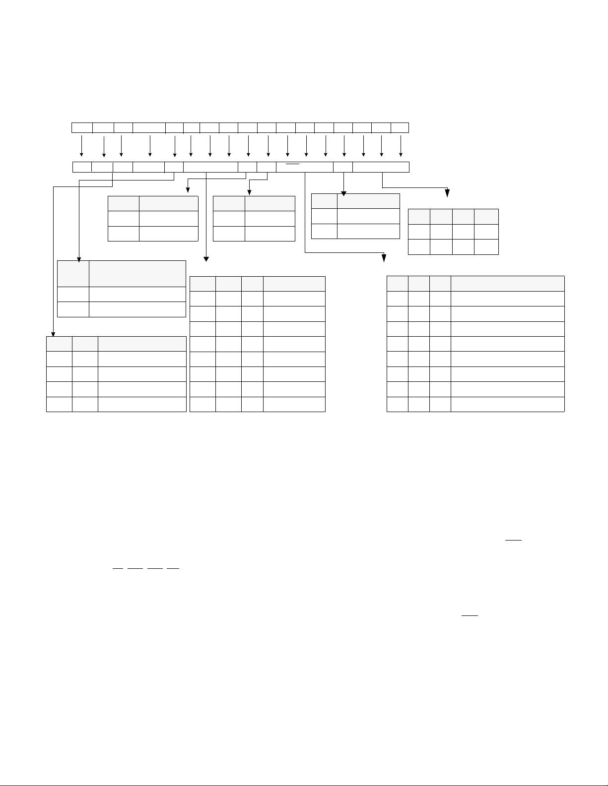
For DDR2 SDRAMs, both bits BA0 and BA1 must be decoded for Mode/Extended Mode Register Set (MRS/EMRS)
commands. Users must initialize all four Mode Registers. The registers may be initialized in any order.
2.3.1 Power-up and initialization sequence
The following sequence is required for Power-up and Initialization.
a) Either one of the following sequence is required for Power-up.
a1) While applying power, attempt to maintain CKE below 0.2 x VDDQ and ODT
*1
at a LOW state (all other inputs
may be undefined.) The VDD voltage ramp time must be no greater than 200 ms from when VDD ramps from
300 mV to VDD min; and during the VDD voltage ramp, |VDD-VDDQ| £ 0.3 volts. Once the ramping of the
supply voltages is complete (when VDDQ crosses VDDQ min), the supply voltage specifications provided in
section 5, Table 16 Recommended DC operating conditions (SSTL_1.8), prevail.
- VDD, VDDL and VDDQ are driven from a single power converter output, AND
- VTT is limited to 0.95 V max, AND
- Vref tracks VDDQ/2, VREF must be within +/- 300 mV with respect to VDDQ/2 during supply ramp time.
- VDDQ
Š VREF must be met at all times.
a2) While applying power, attempt to maintain CKE below 0.2 x VDDQ and ODT
*1
at a LOW state, all other inputs
may be undefined, voltage levels at I/Os and outputs must be less than VDDQ during voltage ramp time to avoid
DRAM latch-up. During the ramping of the supply voltages, VDD Š VDDL Š VDDQ must be maintained and is
applicable to both AC and DC levels until the ramping of the supply voltages is complete, which is when VDDQ
crosses VDDQ min. Once the ramping of the supply voltages is complete, the supply voltage specifications
provided in section 5, Table 16 Recommended DC operating conditions (SSTL_1.8), prevail.
- Apply VDD/VDDL before or at the same time as VDDQ.
- VDD/VDDL voltage ramp time must be no greater than 200 ms from when VDD ramps from 300 mV to VDD
min
- Apply VDDQ before or at the same time as VTT.
- The VDDQ voltage ramp time from when VDD min is achieved on VDD to when VDDQ min is achieved on
VDDQ must be no greater than 500 ms.
(Note: While VDD is ramping, current may be supplied from VDD through the DRAM to VDDQ.)
- Vref must track VDDQ/2, Vref must be within +/- 300 mv with respect to VDDQ/2 during supply ramp time.
- VDDQ Š VREF must be met at all times.
- Apply VTT.
- The VTT voltage ramp time from when VDDQ min is achieved on VDDQ to when VTT min is achieved on VTT
must be no greater than 500 ms.
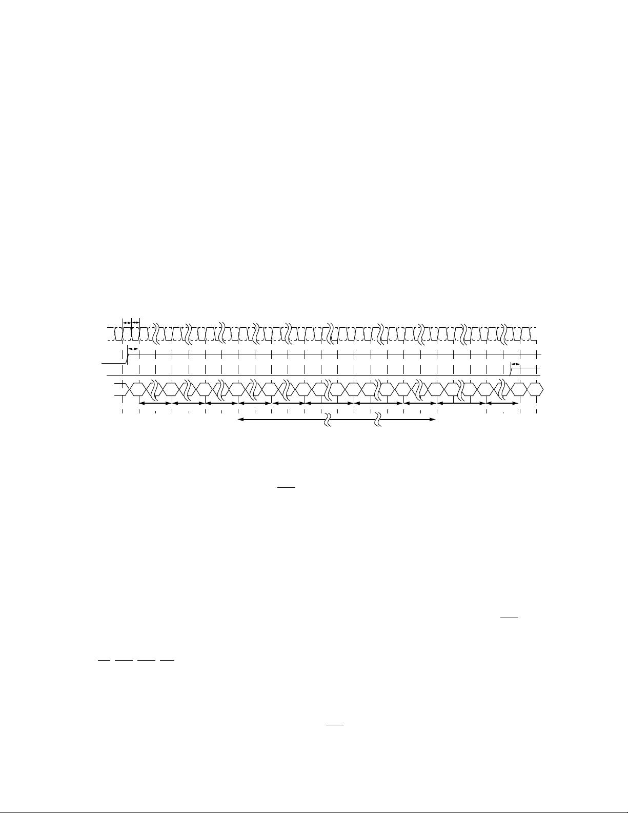
b) Start clock and maintain stable condition.
c) For the minimum of 200 us after stable power (VDD, VDDL, VDDQ, VREF and VTT are between their minimum and
maximum values as stated in section 5, Table 16 Recommended DC operating conditions (SSTL_1.8)) and stable
clock (CK, CK
), then apply NOP or Deselect & take CKE HIGH.
d) Wait minimum of 400 ns then issue precharge all command. NOP or Deselect applied during 400 ns period.
e) Issue an EMRS command to EMR(2). (To issue EMRS command to EMR(2), provide LOW to BA0 and BA2, HIGH
to BA1.)
f) Issue an EMRS command to EMR(3). (To issue EMRS command to EMR(3), provide LOW to BA2, HIGH to BA0
and BA1.)
2 Functional description (cont’d)


