"TLE94108ES 英飞凌芯片中文版规格书手册及特性介绍"
需积分: 5 42 浏览量
更新于2024-01-26
收藏 1.98MB PDF 举报
"TLE94108ES 英飞凌芯片 INFINEON 中文版规格书手册.pdf"描述了英飞凌公司生产的TLE94108ES芯片的特点和功能。该芯片具有八个半桥功率输出,非常低的待机功耗。它的输入兼容3.3V/5V,并带有滞后。所有输出都具有过载和短路保护功能,并且可以独立诊断输出(过电流、开路)。所有高侧和低侧输出在ON状态下都具有开路诊断功能。输出具有可选择的开路阈值(HS1、HS2)。该芯片还配备了具有可选延时环应答能力的16位标准SPI接口,可以进行级联连接。
此规格书手册为使用者提供了关于TLE94108ES芯片的详细说明和说明书,以帮助用户充分了解并正确使用该芯片。它包含了该芯片的主要特点、功能以及技术规格。对于需要使用该芯片进行电路设计或集成到产品中的工程师和设计师来说,这份规格书手册是不可或缺的参考资料。
根据规格书手册的描述,TLE94108ES芯片是一种多功能的功率半桥驱动器。它可以控制和驱动多种类型的负载,如电机、灯光和其他功率驱动电路。该芯片的主要特点是它具有八个独立的半桥功率输出,这意味着它可以同时控制和驱动八个独立的负载。这使得该芯片非常适合用于需要同时控制多个负载的应用,如医疗设备、家庭自动化系统和工业自动化系统。
除了八个半桥输出之外,TLE94108ES芯片还具有其他一些重要的特点。首先,它具有非常低的待机功耗,在待机模式下只消耗极少的能量。这对于需要长时间运行的电池供电应用非常重要,因为它可以延长设备的使用寿命。其次,该芯片的输入兼容3.3V/5V,并具有滞后功能,这使得它可以与不同类型的微控制器和其他设备进行连接。此外,所有输出都具有过载和短路保护功能,可以保护设备免受电流过大或短路引起的损坏。此外,它还具有输出的独立诊断功能,可以检测到过电流和开路等故障。
该规格书手册还介绍了TLE94108ES芯片的接口和通信方式。芯片配备了一个16位标准SPI接口,可以与微控制器或其他外部设备进行通信。此外,该接口还具有级联和延时环应答能力,这意味着多个芯片可以级联连接,以实现更复杂的控制功能。这种灵活的通信方式使得TLE94108ES芯片非常适合用于需要多个芯片协同工作的应用,如机器人控制系统和智能家居系统。
总的来说,TLE94108ES芯片是一款功能强大、多功能的功率半桥驱动器。它具有八个半桥功率输出、低功耗、过载保护和诊断功能,以及灵活的通信接口。它适用于多种应用,包括医疗设备、家庭自动化系统和工业自动化系统。通过阅读规格书手册,使用者可以深入了解该芯片的功能和特性,并有效地将其集成到设计中。
Data Sheet 13 1.0
2020-09-29
TLE94108ES
General Product Characteristics
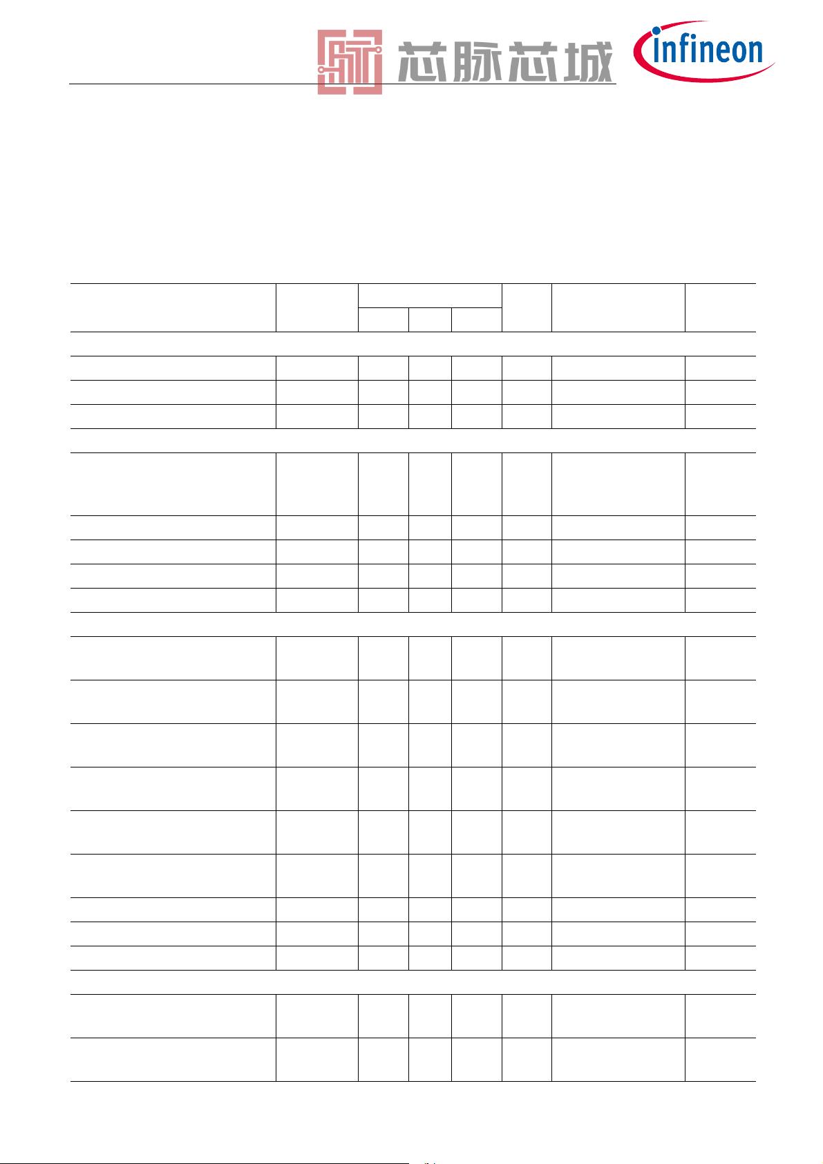
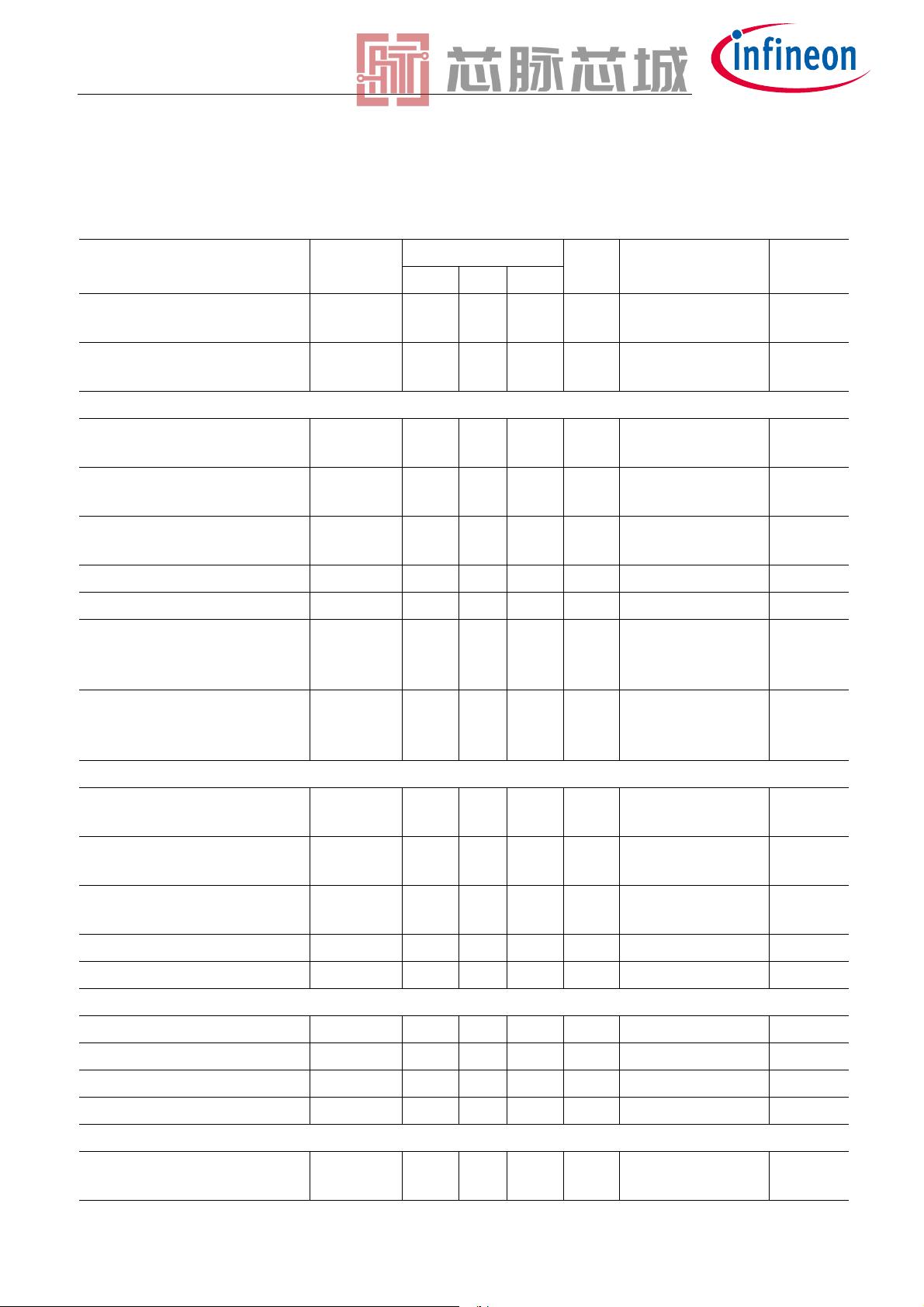
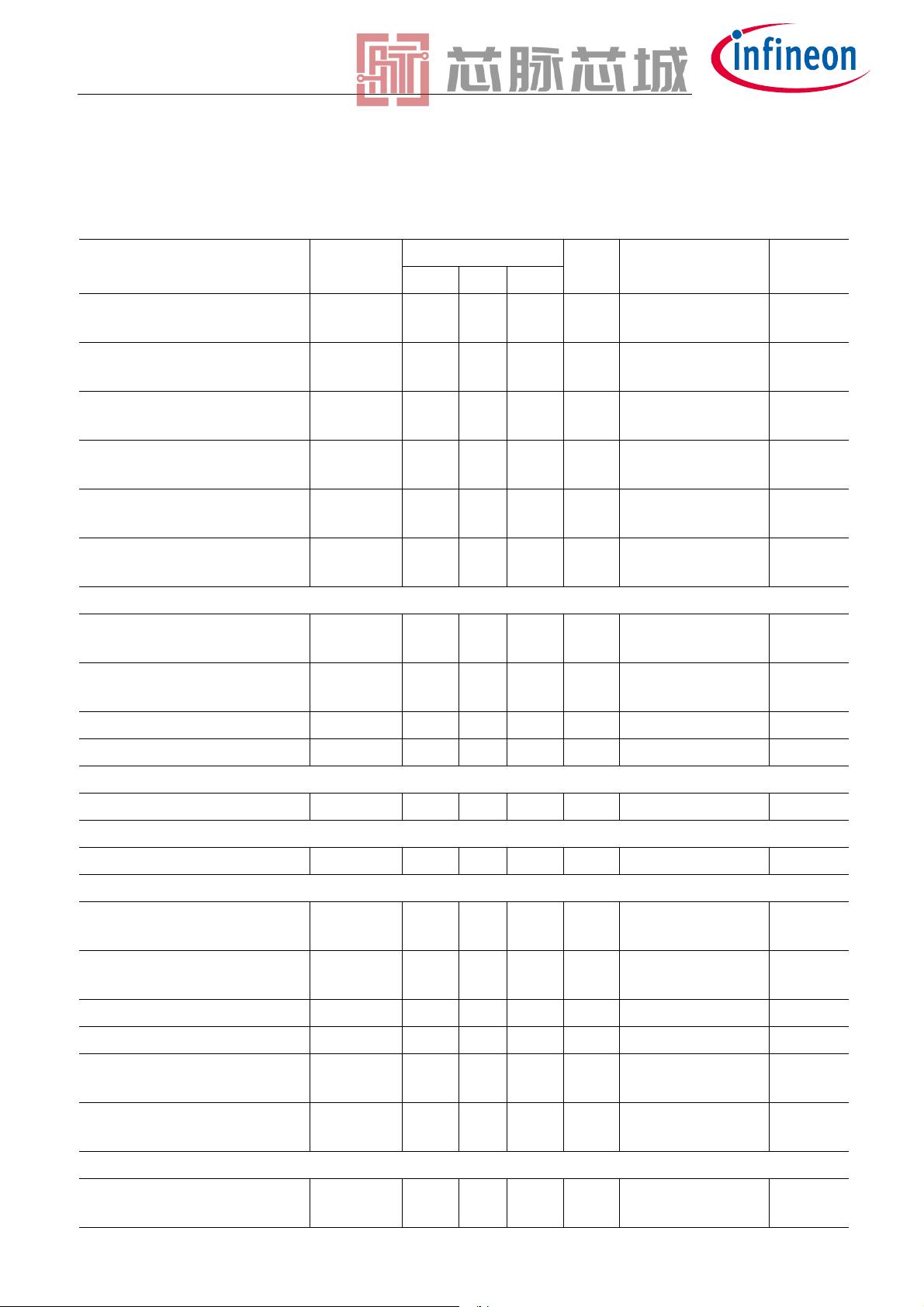
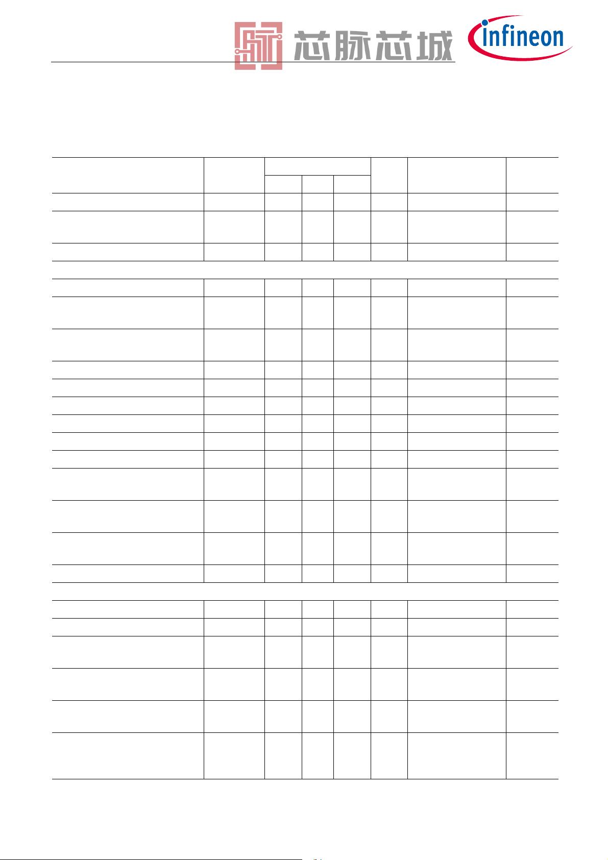
3.4 Electrical Characteristics
Table 5 Electrical Characteristics, V
S
=5.5 V to 18 V, V
DD
= 3.0V to 5.5V, T
j
= -40°C to +150°C, EN= HIGH,
I
OUTn
= 0 A; Typical values refer to V
DD
= 5.0 V, V
S
= 13.5 V and T
J
= 25 °C unless otherwise
specified; all voltages with respect to ground, positive current flowing into pin (unless
otherwise specified)
Parameter Symbol Values Unit Note or
Test Condition
Number
Min. Typ. Max.
Current Consumption, EN = GND
Supply Quiescent current I
SQ
– 0.5 2 µA -40°C ≤ T
j
≤ 85°C P_4.4.1
Logic supply quiescent current I
DD_Q
– 0.1 1 µA -40°C ≤ T
j
≤ 85°C P_4.4.2
Total quiescent current I
SQ
+
I
DD_Q
– 0.6 3 µA -40°C ≤ T
j
≤ 85°C P_4.4.3
Current Consumption, EN=HIGH
Supply current I
S
– 0.5 1 mA Power drivers and
power stages are
off
P_4.4.4
Supply current I
S_HSON
– 4.5 9 mA All high-sides ON
1)
P_4.4.101
Logic supply current I
DD
–1.53mASPI not active P_4.4.5
Logic supply current I
DD_RUN
–5–mASPI 5MHz
3)
P_4.4.6
Total supply current I
S
+
I
DD_RUN
–5.5–mASPI 5MHz
3)
P_4.4.7
Over- and Undervoltage Lockout
Undervoltage Switch ON
voltage threshold
V
UV ON
4.25 – 5.25 V V
S
increasing P_4.4.8
Undervoltage Switch OFF
voltage threshold
V
UV OFF
4–5.0VV
S
decreasing P_4.4.9
Undervoltage Switch ON/OFF
hysteresis
V
UV HY
–0.25–VV
UV ON
- V
UV OFF
3)
P_4.4.10
Overvoltage Switch OFF voltage
threshold
V
OV OFF
21 – 25 V V
S
increasing P_4.4.11
Overvoltage Switch ON voltage
threshold
V
OV ON
20 – 24 V V
S
decreasing P_4.4.12
Overvoltage Switch ON/OFF
hysteresis
V
OV HY
–1–VV
OV OFF
- V
OV ON
3)
P_4.4.13
V
DD
Power-On-Reset V
DD POR
2.40 2.70 2.90 V V
DD
increasing P_4.4.14
V
DD
Power-Off-Reset V
DD POffR
2.35 2.65 2.85 V V
DD
decreasing P_4.4.15
V
DD
Power ON/OFF hysteresis V
DD POR HY
–0.05–VV
DD POR
- V
DD POffR
3)
P_4.4.98
Static Drain-source ON-Resistance (High-Side or Low-Side)
High-Side or Low-Side R
DSON
(all outputs)
R
DSON_HB_25C
– 850 1200 mΩ I
OUT
= ±0.5 A;
T
j
= 25 °C
P_4.4.16
High-Side or Low-Side R
DSON
(all outputs)
R
DSON_HB_150
C
– 1400 1800 mΩ I
OUT
= ±0.5 A;
T
j
= 150 °C
P_4.4.17
剩余75页未读,继续阅读
2023-07-07 上传
2023-07-18 上传
2023-07-07 上传
2023-07-10 上传
2023-07-18 上传
2023-07-07 上传
2023-07-17 上传
2023-07-17 上传

芯脉芯城
- 粉丝: 4
- 资源: 4030
 我的内容管理
展开
我的内容管理
展开


最新资源
- 深入浅出:自定义 Grunt 任务的实践指南
- 网络物理突变工具的多点路径规划实现与分析
- multifeed: 实现多作者间的超核心共享与同步技术
- C++商品交易系统实习项目详细要求
- macOS系统Python模块whl包安装教程
- 掌握fullstackJS:构建React框架与快速开发应用
- React-Purify: 实现React组件纯净方法的工具介绍
- deck.js:构建现代HTML演示的JavaScript库
- nunn:现代C++17实现的机器学习库开源项目
- Python安装包 Acquisition-4.12-cp35-cp35m-win_amd64.whl.zip 使用说明
- Amaranthus-tuberculatus基因组分析脚本集
- Ubuntu 12.04下Realtek RTL8821AE驱动的向后移植指南
- 掌握Jest环境下的最新jsdom功能
- CAGI Toolkit:开源Asterisk PBX的AGI应用开发
- MyDropDemo: 体验QGraphicsView的拖放功能
- 远程FPGA平台上的Quartus II17.1 LCD色块闪烁现象解析
