A Fast-Transient-Response Fully-Integrated Digital
LDO with Adaptive Current Step Size Control
Guigang Cai
1,2
, Chenchang Zhan
1
and Yan Lu
2
1
Department of Electrical and Electronic Engineering, Southern University of Science and Technology, Shenzhen, China
2
The State Key Laboratory of Analog and Mixed-Signal VLSI, University of Macau, Macau, China
Email: caigg@mail.sustc.edu.cn, zhancc@sustc.edu.cn, yanlu@um.edu.mo
Abstract—A 0.6-V 100-mA fully-integrated digital low-
dropout regulator (DLDO) with adaptive current step size control
is presented in this paper. By dividing the main power PMOSs into
ten blocks with different unit-cell sizes, the proposed DLDO can
turn-on/-off small power PMOSs in light load and large ones in
heavy load conditions. High regulation accuracy in a wide load
range and fast transient response are hence achieved. In addition,
an auxiliary power MOS block, which consists of both PMOS and
NMOS transistors, is adopted to eliminate the limit cycle
oscillation (LCO) in light load condition and to further accelerate
the response speed. The proposed DLDO is fabricated in a 65-nm
low-power CMOS technology with an active area of 0.17 mm
2
including an on-chip output capacitor of 1nF. The measured
undershoot and overshoot voltages are only 53 mV and 37 mV,
respectively, when the load current changes between 0 and 100 mA.
The quiescent current is 34.6 μA, while the maximum current
efficiency is 99.96%.
Keywords—digital low-dropout regulator (DLDO), adaptive
current step size control, wide load range, fully-integrated, fast
transient response.
I. INTRODUCTION
Low-dropout regulators (LDOs) are widely used in system-
on-a-chip (SoC) designs for its small voltage ripple, fast
transient response, small area requirement and low cost.
Recently, energy-efficient digital circuits are designed with
near-/sub-threshold supply voltage to reduce the power
consumption. However, low supply voltage brings design
challenges to the traditional analog LDO (ALDO) that consists
of analog amplifiers. Meanwhile, shrinking the channel length
and gate-oxide thickness in advanced CMOS technology
greatly increases the design difficulty of analog circuits.
Therefore, digital LDO (DLDO) was proposed to be an
alternative solution [1], and has attracted enormous attentions.
However, many existing DLDOs suffer from a limited load
current range [1-4], or demand a large decoupling capacitor [5-
6], limiting their applications. Techniques such as reduced
dynamic stability [2], event-driven control [4] and burst mode
technique [5] have been proposed to improve the transient
response, but the effects are not optimal. The analog-assisted
loop scheme in [7] reduces the output variation when the load
current changes from 2 to 12 mA, but is not very effective for a
small initial load current.
In this paper, we present a fully-integrated DLDO with
adaptive current step size control. It achieves wide load range,
good regulation accuracy and fast transient response without
using large quiescent current. In addition, the limit cycle
oscillation (LCO) in light load is alleviated and even eliminated
without a large dead-zone. The working principle and circuit
implementation of the proposed DLDO are discussed in Section
II. Section III shows the measurement results and Section IV
draws the conclusion.
II. OPERATION PRINCIPLE AND CIRCIUT IMPLEMENTATION
A. Operation Principle
DLDO turns on/off one or more power MOSs per clock
cycle to charge/discharge the output voltage V
OUT
to make it
close to the reference voltage V
REF
. However, turning-on/-off
the same power MOS in different load conditions has different
effects on V
OUT
. Specifically, turning-on/-off small‐size power
MOSs is fine in light load but has small effect in heavy load,
which affects the regulation speed. On the other hand, turning-
on/-off large-size power MOSs is OK in heavy load but may lead
to limit cycle oscillation (LCO) and stability problems in light
load. Therefore, we propose to use adaptive power MOS sizes
per load conditions.
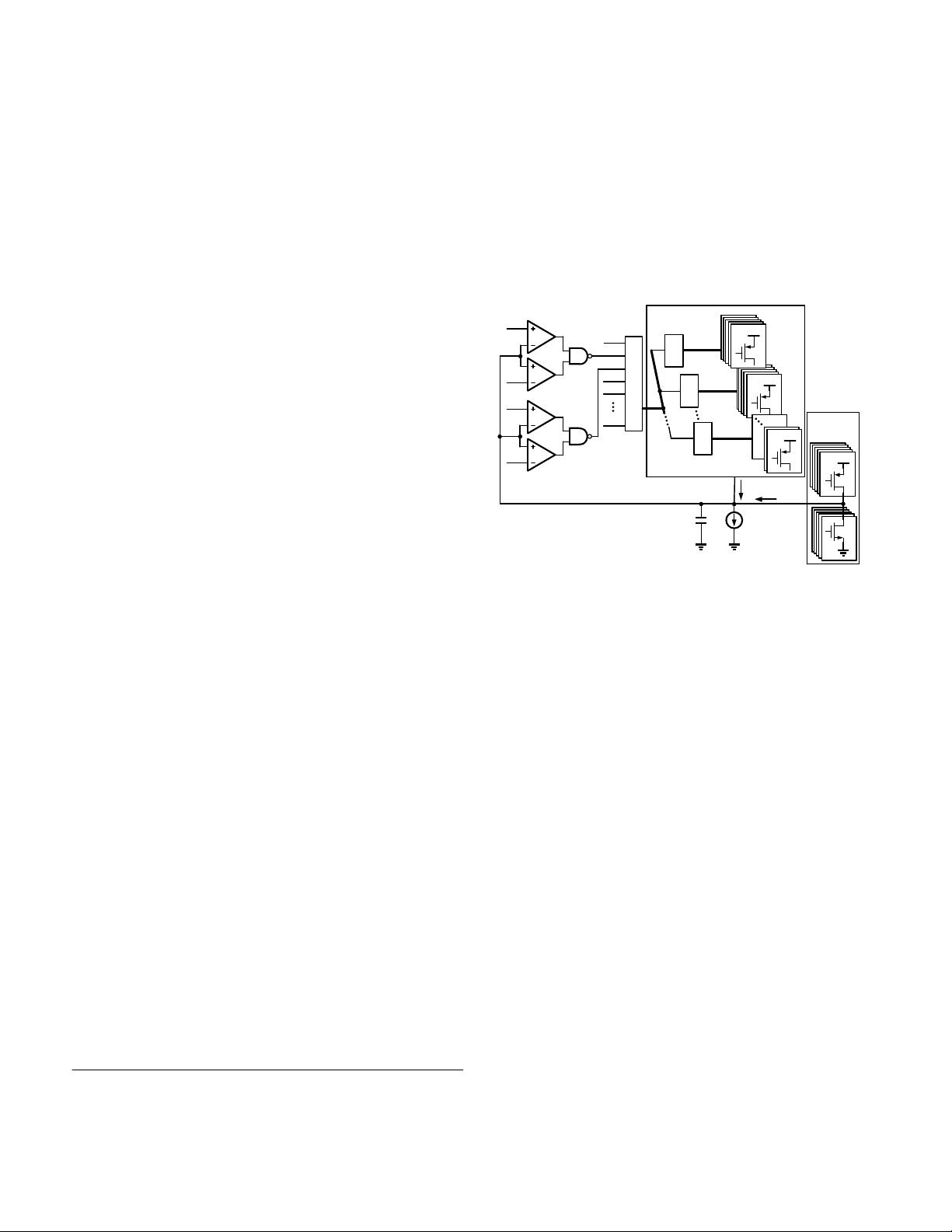
Fig. 1 shows the block diagram of the proposed DLDO,
which consists of 4 comparators, a control circuit, a main power
block, an auxiliary power block, and an output capacitor C
OUT
.
Among the four reference voltages, V
REF+
= V
REF
+ ΔV
1
, V
REF−
= V
REF
- ΔV
1
, V
REFH
= V
REF
+ ΔV
2
and V
REFL
= V
REF
- ΔV
2
, and
ΔV
1
< ΔV
2
. When V
OUT
runs out of the range of [V
REF−
: V
REF+
],
signal EN
1
is set to 1, otherwise EN
1
= 0. Similarly, When V
OUT


