BCM2711外围设备文档:ARM可访问的外设详解
需积分: 9 86 浏览量
更新于2024-06-28
收藏 1.25MB PDF 举报
"BCM2711-peripherals.pdf 是一份技术文档,主要介绍了BCM2711芯片上可由ARM安全访问的各种外围设备,包括定时器、中断控制器、GPIO(通用输入输出)、USB、PCM/I2S(脉冲编码调制/集成电路声音)、DMA(直接存储器访问)控制器、I2C(集成电路总线)主控器、SPI(串行外设接口)主控器、PWM(脉宽调制)和UART(通用异步收发传输器)。这份数据表的目的是为开发者提供足够的信息以便将操作系统移植到BCM2711平台。然而,并非所有外围设备都已完全文档化。还有部分外围设备是设计用来由其他组件控制的。文档由Broadcom Europe Ltd.在2012年首次发布,Raspberry Pi (Trading) Ltd.在2020年进行了更新。"
BCM2711是一款高性能的系统级芯片,广泛应用于嵌入式系统和物联网设备中,特别是Raspberry Pi等单板计算机。该芯片包含了一系列用于处理不同任务的外围接口:
1. **定时器**:定时器是用于精确计时和调度的硬件模块,可以在预设的时间间隔后触发事件或中断。
2. **中断控制器**:中断控制器管理来自各种设备的中断请求,确保处理器能及时响应外部事件。
3. **GPIO**:GPIO接口允许芯片与外部设备进行双向数字通信,通过编程设置引脚为输入或输出模式。
4. **USB**:USB接口支持高速数据传输,用于连接键盘、鼠标、打印机、存储设备等外围设备。
5. **PCM/I2S**:这些接口用于音频数据的传输,常用于连接音频编解码器和数字音频设备。
6. **DMA控制器**:DMA控制器可以绕过CPU直接在内存和外设之间传输数据,提高数据传输效率。
7. **I2C主控器**:I2C是一种多设备串行总线,用于低速、低功耗的设备间通信。
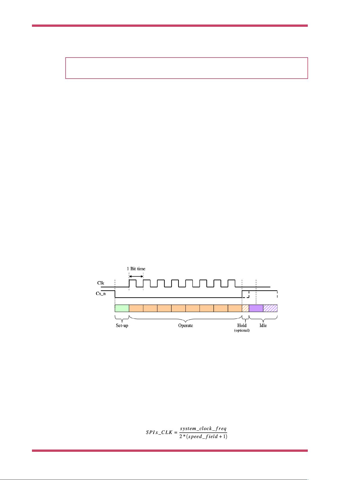
8. **SPI主控器**:SPI接口支持高速全双工通信,适用于传感器、显示屏等高速数据交换的场合。
9. **PWM**:PWM用于生成模拟信号,常见应用包括LED亮度调节、电机速度控制等。
10. **UARTs**:UART接口用于异步串行通信,常见于串口调试和与其他设备的通信。
文档还提到了地址映射、外围设备访问的内存顺序注意事项,以及如UART1、SPI1、SPI2等辅助设备的详细信息,包括它们的实现细节、寄存器描述和功能。例如,MiniUART是一个简化版的UART,适用于轻量级通信;而Universal SPI Master提供了两个SPI接口,支持长位流传输和中断功能。
BCM2711的文档还涵盖了BSC(Burst Serial Controller),可能是I2C协议的一个变种,用于与其他I2C兼容设备交互。每个外围设备部分都包含了对其工作原理、操作方式和相关寄存器的详细描述,这对于开发者理解和驱动这些硬件是至关重要的。
这份文档是开发基于BCM2711平台的软件或硬件设计的重要参考资料,它提供了从底层硬件层面理解和操作这些外围设备所需的详细信息。对于想要移植操作系统或编写驱动程序的开发者来说,是不可或缺的工具。
Receiver enable
If this bit is clear no new symbols will be accepted by the receiver. Any symbols in progress of reception will be
finished.
Transmitter enable
If this bit is clear no new symbols will be sent by the transmitter. Any symbols in progress of transmission will be
finished.
Auto flow control
Automatic flow control can be enabled independent for the receiver and the transmitter.
CTS auto flow control impacts the transmitter only. The transmitter will not send out new symbols when the CTS line is
de-asserted. Any symbols in progress of transmission when the CTS line becomes de-asserted will be finished.
RTS auto flow control impacts the receiver only. In fact the name RTS for the control line is incorrect and should be RTR
(Ready to Receive). The receiver will de-assert the RTS (RTR) line when its receive FIFO has a number of empty spaces
left. Normally 3 empty spaces should be enough.
If looping back a mini UART using full auto flow control the logic is fast enough to allow the RTS auto flow level of '10' (De-
assert RTS when the receive FIFO has 1 empty space left).
Auto flow polarity
To offer full flexibility the polarity of the CTS and RTS (RTR) lines can be programmed. This should allow the mini
UART to interface with any existing hardware flow control available.
AUX_MU_STAT_REG Register
Description
The AUX_MU_STAT_REG provides a lot of useful information about the internal status of the mini UART not found on
a normal 16550 UART.
Table 14.
AUX_MU_STAT_REG
Register
Bits Name Description Type Reset
31:28 Reserved. - - -
27:24 Transmit FIFO fill
level
These bits shows how many symbols are stored in the
transmit FIFO
The value is in the range 0-8
RO 0x0
23:20 Reserved. - - -
19:16 Receive FIFO fill
level
These bits shows how many symbols are stored in the
receive FIFO
The value is in the range 0-8
RO 0x0
15:10 Reserved. - - -
9 Transmitter done This bit is set if the transmitter is idle and the transmit FIFO
is empty.
It is a logic AND of bits 3 and 8
RO 0x1
8 Transmit FIFO is
empty
If this bit is set the transmitter FIFO is empty. Thus it can
accept 8 symbols.
RO 0x1
7 CTS line This bit shows the status of the UART1_CTS line. RO 0x0
6 RTS status This bit shows the status of the UART1_RTS line. RO 0x0
5 Transmit FIFO is
full
This is the inverse of bit 1 RO 0x0
BCM2711 ARM Peripherals
2.2. Mini UART 15


剩余163页未读,继续阅读
2021-03-28 上传
2021-01-04 上传
2020-05-23 上传
2016-03-11 上传
2014-11-14 上传
2021-10-02 上传

这个网友未命名
- 粉丝: 1
- 资源: 14
 我的内容管理
展开
我的内容管理
展开


最新资源
- R语言中workflows包的建模工作流程解析
- Vue统计工具项目配置与开发指南
- 基于Spearman相关性的协同过滤推荐引擎分析
- Git基础教程:掌握版本控制精髓
- RISCBoy: 探索开源便携游戏机的设计与实现
- iOS截图功能案例:TKImageView源码分析
- knowhow-shell: 基于脚本自动化作业的完整tty解释器
- 2011版Flash幻灯片管理系统:多格式图片支持
- Khuli-Hawa计划:城市空气质量与噪音水平记录
- D3-charts:轻松定制笛卡尔图表与动态更新功能
- 红酒品质数据集深度分析与应用
- BlueUtils: 经典蓝牙操作全流程封装库的介绍
- Typeout:简化文本到HTML的转换工具介绍与使用
- LeetCode动态规划面试题494解法精讲
- Android开发中RxJava与Retrofit的网络请求封装实践
- React-Webpack沙箱环境搭建与配置指南
