This article has been accepted for inclusion in a future issue of this journal. Content is final as presented, with the exception of pagination.
2 IEEE JOURNAL OF SOLID-STATE CIRCUITS
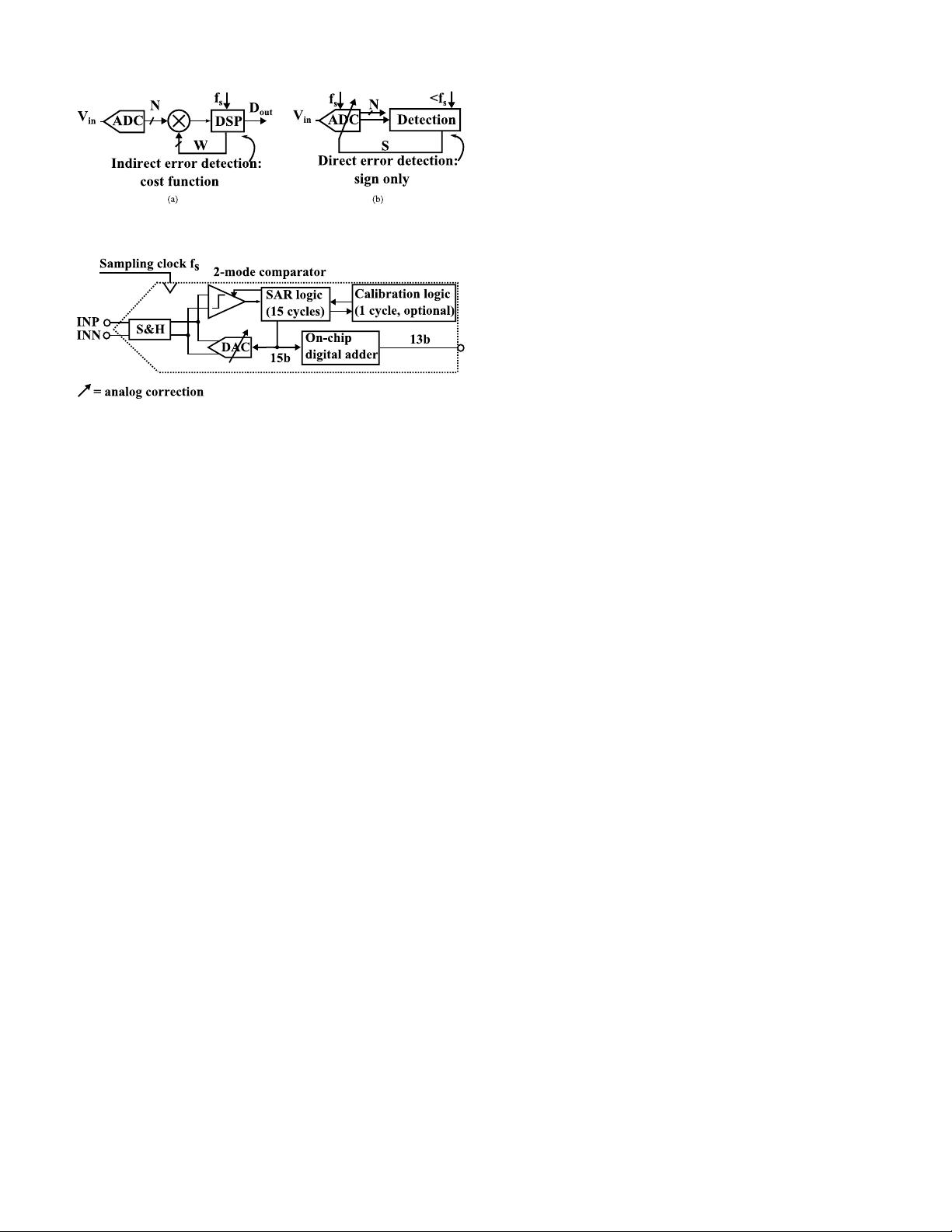
Fig. 1. (a) Block diagram of the prior arts’ calibration method and
(b) proposed calibration method for a N bit ADC.
Fig. 2. Block diagram of a 13 b SAR ADC.
In prior art, without knowing any information of the error,
often the circuit errors are corrected indirectly in a digital
fashion [2], [3], [10] via postprocessing. Fig. 1(a) shows the
block diagram of the calibration method in [2], [3], and [10].
Based on the ADC output data, a DSP engine can define a
cost function, which reflects the error. Through an adaptive
algorithm, e.g., LMS, the value of the cost function will
be tuned toward zero once the coefficients W are correctly
trained. To guarantee the precision of the coefficient training,
redundancy is usually introduced in the DSP engine. On the
other hand, a direct error detection and correction scheme is
proposed as shown in Fig. 1(b). The sign of error can be
detected as shown later. Thanks to the feedback loop and the
analog correction circuit, it is very convenient to stepwise
tune the error toward zero based on its sign. In this way,
only the sign needs to be processed compared with the whole
ADC output in Fig. 1(a). Besides, power-hungry operations
[e.g., multiplying in Fig. 1(a)] are avoided and only much
simpler calculations (e.g., accumulation) are needed. Further-
more, instead of a blind algorithm requiring many iterations,
the sign of the individual errors can be directly detected to
compensate these errors, reducing the convergence time and
required energy. Moreover, the actual correction is in analog
domain instead of digital signal processing as shown later,
consuming far less power. Overall, the proposed calibration
method has very little overhead in circuit complexity, area,
speed, and power.
A. ADC Architecture
Fig. 2 shows the architecture of the 13 b SAR ADC.
In each SAR conversion, first, the S&H samples the differ-
ential analog input voltage on the capacitor arrays inside the
DAC. Using the comparator and the logic, the DAC output
will approximate the sampled input voltage in several com-
parisons through a successive-approximation algorithm using
a monotonic switching scheme [16]. In this design, a total of
15 cycles is used to perform a 13 b conversion, where two of
them are redundant cycles to overcome various errors during
the conversion (e.g., DAC settling and noise), similar to [14].
The 13 b output is calculated from the 15 b raw code by an
on-chip digital adder. A two-mode comparator is introduced
to save power while still maintaining accuracy. Optionally, an
additional (16
th
) cycle can be activated for DAC mismatch
calibration or comparator offset calibration as shown later. All
the operations including the calibrations are asynchronously
controlled. Thus, only one relatively low-frequency sampling
clock f
s
is needed for both normal operation and calibration.
Fig. 3 shows the conversion scheme as well as the DAC of
the 13 b ADC. The 15 cycles include ten coarse cycles and
five fine cycles, where the 7
th
and 11
th
cycle are the redundant
cycles. The first redundant bit (7
th
cycle) relaxes DAC settling
time and facilitates the DAC mismatch calibration, which will
be explained later. Considering that the worst mismatch errors
happen for the largest capacitors, only the first five DAC
capacitors are calibrated in this paper. The capacitors lower
than the redundant bit are not calibrated; thus, they need to be
sufficiently linear intrinsically. Thanks to the second redundant
bit (11
th
cycle), a two-mode comparator can be employed [14].
This redundancy allows, first of all, the decision errors during
the coarse comparisons due to the comparator noise, thus
allowing a low-power mode comparator. Furthermore, since
the redundancy can tolerate the residual comparator offset
error after calibration as shown later, the comparator offset
calibration accuracy can be relaxed. The combination of
postcalibration comparator offset and coarse comparator noise
should remain within the redundancy range of the 11
th
bit,
which can tolerate errors up to ±8LSB.
B. Comparator Offset Error Detection
As mentioned earlier, the comparator works in the low-
power mode for the first cycles (coarse cycles), and it
only switches to the low-noise mode with higher power for
the last few cycles (fine cycles). In this way, the overall
power consumption of the comparator is reduced while it
still satisfies the noise requirement of the ADC. However,
the two-mode comparator will have two different offsets for
the corresponding two modes. Once this dynamic offset is
beyond the redundancy range (±8LSB), the ADC performance
cannot be recovered. Therefore, calibration of the dynamic
offset becomes necessary. The goal of the comparator offset
calibration is to minimize the offset difference V
delta
,which
equals V
off1
–V
off2
. Since a feedback loop [Fig. 1(b)] is used
to minimize V
delta
stepwise, rather than post processing, it is
sufficient to detect the sign of V
delta
only in order to minimize
its value.
The comparator dynamic offset detection is shown in Fig. 4.
The equivalent voltage at the comparator input V
eq
can be
viewed as a summation of the sampled input signal V
in
, DAC
reference voltage (V
DAC
), and the input-referred comparator
offset [V
off1(2)
]. The optional additional (16
th
) cycle is per-
formed on top of the 15-cycle comparison for a 13 b ADC.
The same comparison as the last (15
th
) cycle is repeated in
the additional (16
th
) cycle. The DAC code remains unchanged,
but the comparator switches from mode2 to mode1.Ideally,if
the two offsets are the same, the comparison result of the
last cycle (D
15
) and the additional cycle (D
16
) would be the
same. However, if the offsets are different, then the equivalent


