A 1V 830μW Full-band ZigBee Receiver Front-end
with Current-reuse and G
m
-boosting Techniques
*
Zengqi Wang, Zhiqun Li
Institute of RF- & OE-ICs Southeast University
Nanjing, China
Email: zhiqunli@seu.edu.cn
Zengqi Wang, Zhiqun Li
Jiangsu Provincial Key Laboratory of Sensor Network Technology
Wuxi, China
Email: zhiqunli@seu.edu.cn
Abstract—A low-voltage low-power CMOS ZigBee receiver
front-end supporting 780/868/915/2400MHz bands is presented in
this paper. 7
he wideband common-gate (CG) low noise amplifier
(LNA) and the I/Q current-commutating mixer are merged in a
single circuit, sharing the bias current. Active trans-conductance
(g
m
) boosting technique is utilized in the design of the presented
receiver front-end. The topology and optimization method of the
presented front-end are shown. Post-layout simulation results for
180nm RF CMOS implementations show the conversion gain is
26.5dB at 780/868/915MHz bands and 19.5dB at 2400MHz band.
The minimum simulated NF is 6.5dB. The receiver front-end
consumes 830μW from a 1V DC supply and the active size of core
circuit is 0.0276mm
2
.
Keywords—low-voltage; low-power; CMOS; ZigBee; current-
reuse; full-band; receiver front-end
I. INTRODUCTION
Recently, low voltage and low power consumption is
increasingly becoming one of the big trends in wireless
communication systems. The ZigBee communication standard
built on top of IEEE 802.15.4 for wireless personal area
networks (WPAN) is being adopted by applications with long
battery lifetime and low transmission data rata. The
specifications relax the requirements on the RF receiver front-
end and create demand for ultra-low-power (ULP) designs [1].
Several ULP receivers have been reported [2-4]. As the
need of high Q off-chip RF filter is eliminated, low-IF and
zero-IF are two typical architectures in ULP receiver designs.
Zero-IF architecture has minimized the hardware overhead of
the RF receiver. However, it usually suffers from DC offset,
high flicker noise, LO leakage, even-order distortion and I/Q
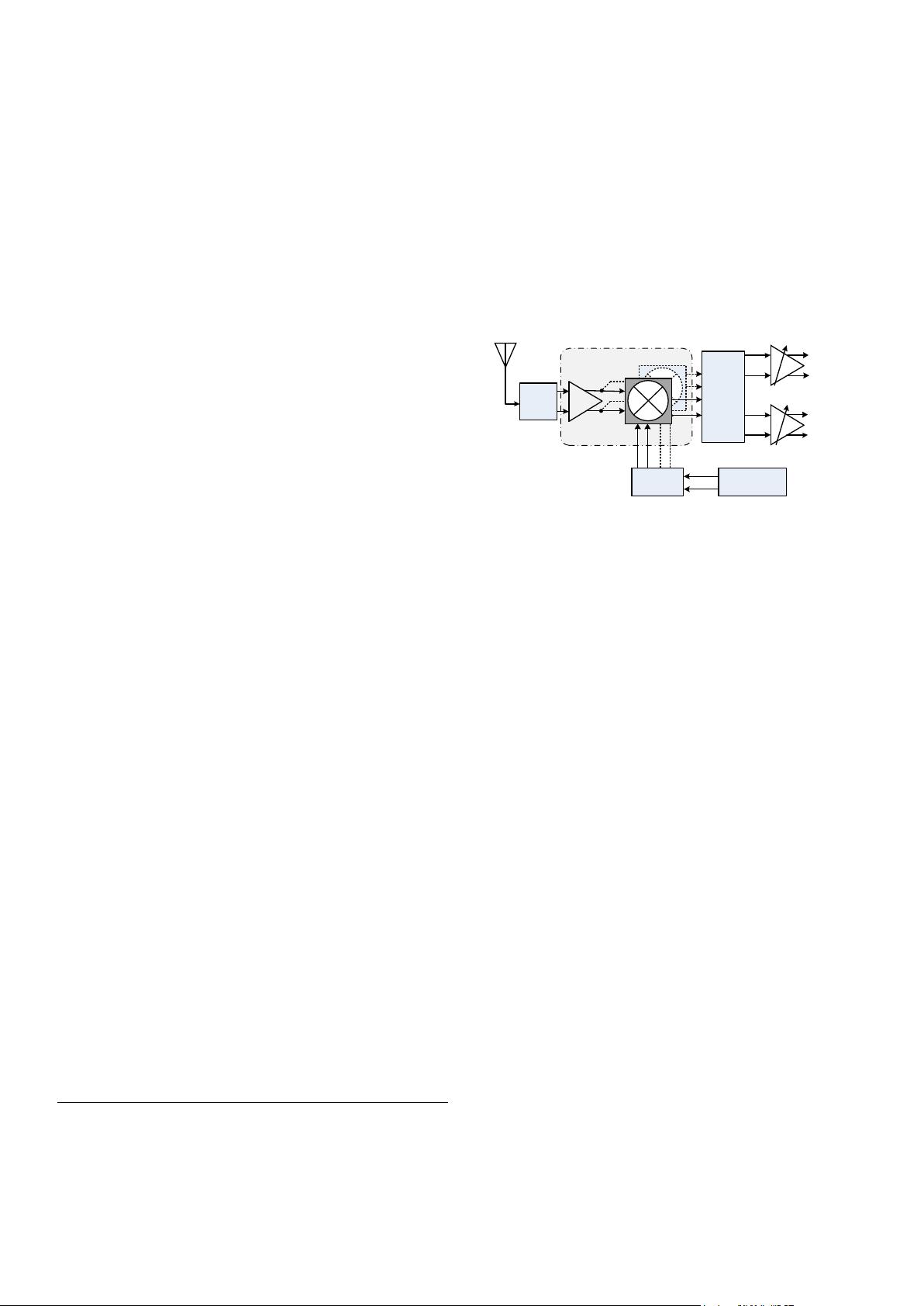
mismatch [2]. As shown in Fig. 1, the receiver presented in
this paper employs the low-IF architecture in order to avoid
the drawbacks mentioned above. The receiver front-end
accepts the weak signal from the antenna for amplification and
converts the sub-GHz RF signal to 2MHz IF signal. The
complex band-pass filter following by the front-end can
suppress the image signal and out-of-band interferences.
As the first active stage of RF receiver, front-end plays a
critical role in the overall performance. The design of receiver
front-end is a tradeoff among the power consumption,
conversion gain, noise figure, input match and linearity.
Various kinds of topologies and techniques have been
introduced to optimize the performance of the front-end.
Literature [2] published a ULP receiver front-end composed of
a two-stage capacitor-cross-coupled (CCC) CG-LNA and a
quadrature Gilbert I/Q mixer. Although the current-reuse and
g
m
-boosting techniques have been applied in the circuit design,
the bias current for LNA and mixer are separate and can’t be
reduced any further. The LNA-Mixer-VCO (LMV) cell was
presented in [3]. Sharing the bias current among LNA, Mixer
and VCO save the power successfully. However, the NF and
input match S
11
are sensitive to its external high-Q inductor for
narrowband input match and passive pre-gain. Also, under the
single bias current, it’s hard to optimize the LNA’s NF and the
VCO’s phrase noise at the same time. With less voltage
headroom, the LMV cell is not suitable for the low voltage
applications. To reserve more voltage headroom for the
dynamic range, one more design of current-reuse receiver
front-end merging the LNA and baseband (BB) trans-
impedance amplifier (TIA) was reported in [4]. The LNA and
the TIA are biased with the same current. However, the
LNA’s NF should benefit from short-channel length of the
MOSFETs while the BB TIA preferring long-channel ones to
reduce the flicker noise.
In this paper, a ZigBee receiver front-end exploiting RF-
to-BB current-reuse topology is proposed, which can
effectively restrain the power consumption, enhance the
conversion gain and reduce the noise simultaneously. As
shown in Fig.2, the wideband CG LNA and I/Q current-
commutating mixer are merged in a single circuit, sharing the
bias current. A divide-by-two circuit and LO buffers generate
the quadrature LO signals for I/Q mixers from the LO
ext
. Two
50Ω buffers are integrated on chip for test.
*Project supported by the
National Natural Science Foundation of China
(No. 61474021)
.
978-1-4799-8893-8/15/$31.00 ©2015 IEEE
Balun
Antenna
LNA
DIV/2
BPF
PGA
I
Q
Q-Mixer
I-Mixer
Current-reuse Front-end
ZigBee Receiver
PLL
Fig.1 Block diagram of the proposed ZigBee receiver.


