Micromachines 2020, 11, 222 3 of 11
the device was 2
µ
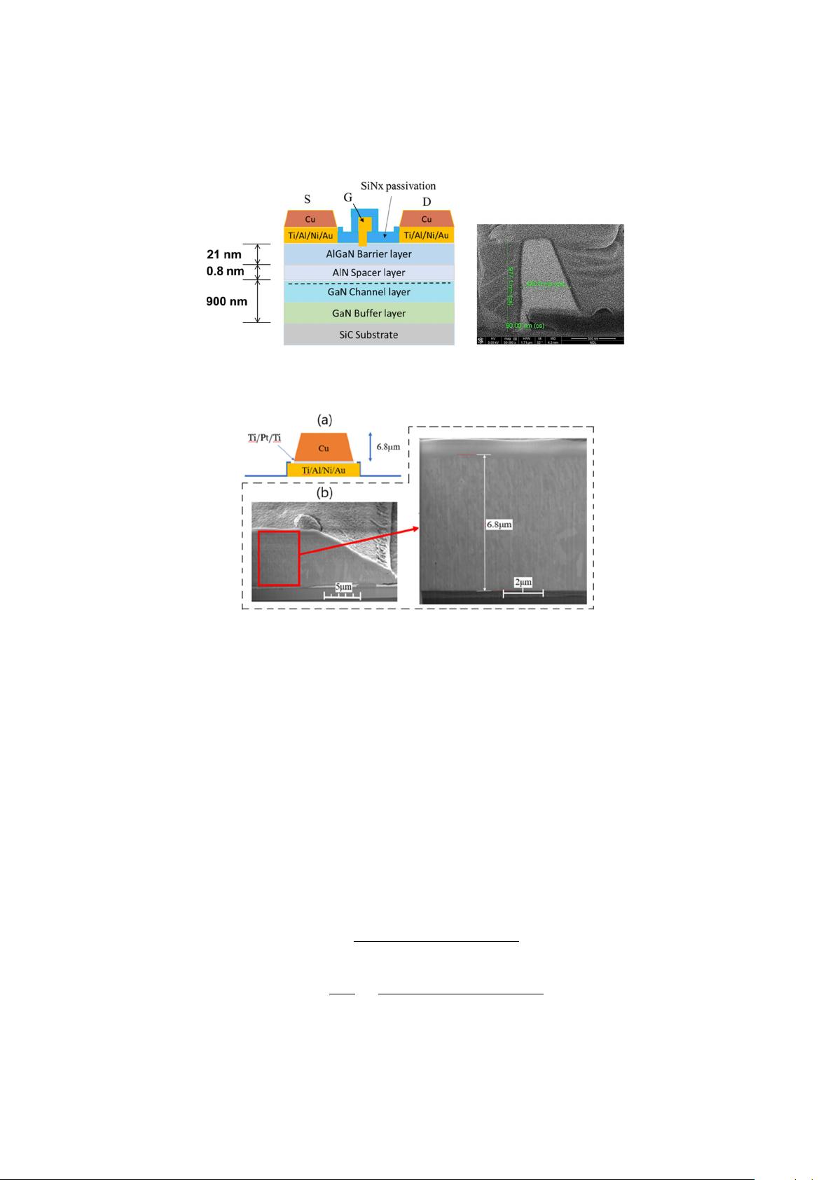
m with the gate positioned at the center. The schematic of thick copper metallization
technology and the SEM image of thick copper metallization cross-section are shown in Figure 2.
Micromachines 2020, 11, x 3 of 11
metallization technology and the SEM image of thick copper metallization cross-section are shown
in Figure 2.
Figure 1. AlGaN/GaN high-electron-mobility transistors (HEMTs) epitaxial configuration and device
structure with scanning electron microscope (SEM) image of the gate.
Figure 2. (a) Schematic of thick copper metallization structure. (b) SEM image of cross-section of thick
copper metallization for GaN HEMT.
3. Results and Discussions
The two-port network analysis method with a small signal model was used to analyze the
relationship between the drain–source current (I
DS
) and the transconductance (G
m
) versus source
resistance and drain resistance. The DC and RF measurement results of devices with and without
thick copper metallization were then compared. By utilizing load-pull measurement methodology,
output power and power-added efficiency (PAE) characteristics could be obtained [16]. The impact
of gate width on the device performance are then able to be discussed.
3.1. Two-Port Network Analysis
With a two-port network, the small signal model of the AlGaN/GaN HEMT device can be
depicted as in Figure 3 [17,18]. Utilizing the y-parameter analysis, the drain–source current (I
DS
) and
the transconductance (G
m
) of the device can be derived as:
𝐼
𝑦
𝑣
𝑦
𝑣
1𝑦
𝑅
𝑦
𝑅
𝑦
𝑅
(1)
𝐺
𝑑𝐼
𝑑𝑣
𝑦
1𝑦
𝑅
𝑦
𝑅
𝑦
𝑅
(2)
It is apparent from Equations (1) and (2) that the decrease of R
S
' and R
D
' results in the increase of
I
DS
and G
m
levels.
Figure 1.
AlGaN/GaN high-electron-mobility transistors (HEMTs) epitaxial configuration and device
structure with scanning electron microscope (SEM) image of the gate.
Micromachines 2020, 11, x 3 of 11
metallization technology and the SEM image of thick copper metallization cross-section are shown
in Figure 2.
Figure 1. AlGaN/GaN high-electron-mobility transistors (HEMTs) epitaxial configuration and device
structure with scanning electron microscope (SEM) image of the gate.
Figure 2. (a) Schematic of thick copper metallization structure. (b) SEM image of cross-section of thick
copper metallization for GaN HEMT.
3. Results and Discussions
The two-port network analysis method with a small signal model was used to analyze the
relationship between the drain–source current (I
DS
) and the transconductance (G
m
) versus source
resistance and drain resistance. The DC and RF measurement results of devices with and without
thick copper metallization were then compared. By utilizing load-pull measurement methodology,
output power and power-added efficiency (PAE) characteristics could be obtained [16]. The impact
of gate width on the device performance are then able to be discussed.
3.1. Two-Port Network Analysis
With a two-port network, the small signal model of the AlGaN/GaN HEMT device can be
depicted as in Figure 3 [17,18]. Utilizing the y-parameter analysis, the drain–source current (I
DS
) and
the transconductance (G
m
) of the device can be derived as:
𝐼
𝑦
𝑣
𝑦
𝑣
1𝑦
𝑅
𝑦
𝑅
𝑦
𝑅
(1)
𝐺
𝑑𝐼
𝑑𝑣
𝑦
1𝑦
𝑅
𝑦
𝑅
𝑦
𝑅
(2)
It is apparent from Equations (1) and (2) that the decrease of R
S
' and R
D
' results in the increase of
I
DS
and G
m
levels.
Figure 2.
(
a
) Schematic of thick copper metallization structure. (
b
) SEM image of cross-section of thick
copper metallization for GaN HEMT.
3. Results and Discussions
The two-port network analysis method with a small signal model was used to analyze the
relationship between the drain–source current (I
DS
) and the transconductance (G
m
) versus source
resistance and drain resistance. The DC and RF measurement results of devices with and without thick
copper metallization were then compared. By utilizing load-pull measurement methodology, output
power and power-added efficiency (PAE) characteristics could be obtained [
16
]. The impact of gate
width on the device performance are then able to be discussed.
3.1. Two-Port Network Analysis
With a two-port network, the small signal model of the AlGaN/GaN HEMT device can be depicted
as in Figure 3 [
17
,
18
]. Utilizing the y-parameter analysis, the drain–source current (I
DS
) and the
transconductance (G
m
) of the device can be derived as:
I
DS
=
y
21
v
0
i
+ y
22
v
0
o
1 + y
21
R
0
S
+ y
22
R
0
S
+ y
22
R
0
D
(1)
G
m
=
dI
DS
dv
0
i
=
y
21
1 + y
21
R
0
S
+ y
22
R
0
S
+ y
22
R
0
D
(2)


