

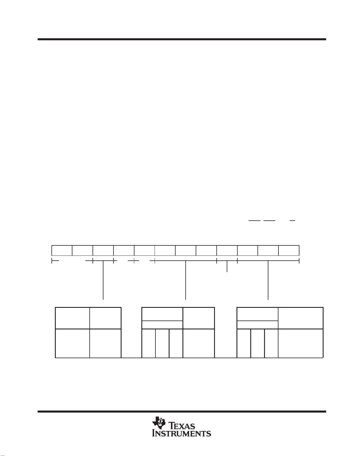
TMS626162
524288 BY 16-BIT BY 2-BANK
SYNCHRONOUS DYNAMIC RANDOM-ACCESS MEMORY
SMOS683E – FEBRUARY 1995 – REVISED APRIL 1997
8
POST OFFICE BOX 1443 • HOUSTON, TEXAS 77251–1443
two-bank row-access operation
The two-bank feature allows access of information on random rows at a higher rate of operation than is possible
with a standard DRAM, by activating one bank with a row address and, while the data stream is being accessed
to/from that bank, activating the second bank with another row address. When the data stream to or from the
first bank is complete, the data stream to or from the second bank can begin without interruption. After the
second bank is activated, the first bank can be deactivated to allow the entry of a new row address for the next
round of accesses. In this manner, operation can continue in an interleaved fashion. Figure 28 is an example
of two-bank row-interleaving read bursts with automatic deactivate for a CAS latency of three and burst length
of eight.
two-bank column-access operation
The availability of two banks allows the access of data from random starting columns between banks at a higher
rate of operation. After activating each bank with a row address (ACTV command), A11 can be used to alternate
READ or WRT commands between the banks to provide gapless accesses at the CLK frequency, provided all
specified timing requirements are met. Figure 29 is an example of two-bank column-interleaving read bursts
for a CAS latency of three and burst length of two.
bank deactivation (precharge)
Both banks can be deactivated (placed in precharge) simultaneously by using the DCAB command. A single
bank can be deactivated by using the DEAC command. The DEAC command is entered identically to the DCAB
command except that A10 must be low and A11 used to select the bank to be precharged as shown in Table 1.
A bank can be deactivated automatically by using A10 during a read or write command. If A10 is held high during
the entry of a read or write command, the accessed bank (selected by A11) is deactivated automatically upon
completion of the access burst. If A10 is held low during the entry of a read or write command, that bank remains
active following the burst. The read and write commands with automatic deactivation are signified as READ-P
and WRT-P.
chip select (CS)
CS can be used to select or deselect the ’626162 for command entry, which might be required for
multiple-memory-device decoding. If CS
is held high on the rising edge of CLK (DESL command), the device
does not respond to RAS
, CAS, or W until the device is selected again by holding CS low on the rising edge
of CLK. Any other valid command can be entered simultaneously on the same rising CLK edge of the select
operation. The device can be selected/deselected on a cycle-by-cycle basis (see Table 1 and Table 2). The use
of CS
does not affect an access burst that is in progress; the DESL command can only restrict RAS, CAS, and
W
input to the ’626162.
data mask
The mask command or its opposite, the data-in enable (ENBL) command (see Table 3), is performed on a
cycle-by-cycle basis to gate any data cycle within a read burst or a write burst. DQML controls DQ0–DQ7, and
DQMU controls DQ8–DQ15. The application of DQMx to a write burst has no latency (n
DID
= 0 cycle), but the
application of DQMx to a read burst has a latency of n
DOD
= 2 cycles. During a write burst, if DQMx is held high
on the rising edge of CLK, the data-input is ignored on that cycle. During a read burst, if DQMx is held high on
the rising edge of CLK and n
DOD
cycles after that rising edge of CLK, the data-output is in the high-impedance
state. Figure 18 and Figure 32 through Figure 35 show examples of data-mask operation.
剩余43页未读,继续阅读

不觉明了
- 粉丝: 3271
- 资源: 5614
 我的内容管理
收起
我的内容管理
收起
- 我的资源
快来上传第一个资源
 我的收益 登录查看自己的收益
 我的积分
登录查看自己的积分
我的积分
登录查看自己的积分
 我的C币
登录后查看C币余额
我的C币
登录后查看C币余额
 我的收藏
我的收藏  我的下载
我的下载  下载帮助
下载帮助

会员权益专享


最新资源
- VMP技术解析:Handle块优化与壳模板初始化
- C++ Primer 第四版更新:现代编程风格与标准库
- 计算机系统基础实验:缓冲区溢出攻击(Lab3)
- 中国结算网上业务平台:证券登记操作详解与常见问题
- FPGA驱动的五子棋博弈系统:加速与创新娱乐体验
- 多旋翼飞行器定点位置控制器设计实验
- 基于流量预测与潮汐效应的动态载频优化策略
- SQL练习:查询分析与高级操作
- 海底数据中心散热优化:从MATLAB到动态模拟
- 移动应用作业:MyDiaryBook - Google Material Design 日记APP
- Linux提权技术详解:从内核漏洞到Sudo配置错误
- 93分钟快速入门 LaTeX:从入门到实践
- 5G测试新挑战与罗德与施瓦茨解决方案
- EAS系统性能优化与故障诊断指南
- Java并发编程:JUC核心概念解析与应用
- 数据结构实验报告:基于不同存储结构的线性表和树实现
资源上传下载、课程学习等过程中有任何疑问或建议,欢迎提出宝贵意见哦~我们会及时处理!
点击此处反馈


