A Novel Level-Shifter Integrated on the Edge
Termination Region of the High Voltage Device
Jiayu Wu, Xinjiang Lyu, Moufu Kong, Bo Yi and Xingbi Chen, Life Senior Member, IEEE
State Key Laboratory of Electronic Thin Films and Integrated Devices
University of Electronic Science and Technology of China
Chengdu, China
wujiayu_uestc@163.com;
Abstract—A novel level-shifter consisting of one LDMOS and
one P-i-N diode integrated on the High Voltage Edge
Termination (HVET) region in the high-side region is proposed.
Thus the area of the level-shifter is saved, and the
interconnection-induced pre-breakdown is avoided. The
simulation results verify the required level-shifting function of
the integrated structure.
Keywords—HVIC; level-shifter; isolation; LDMOS; P-i-N
diode
I. INTRODUCTION
HVIC is widely used for motor control application,
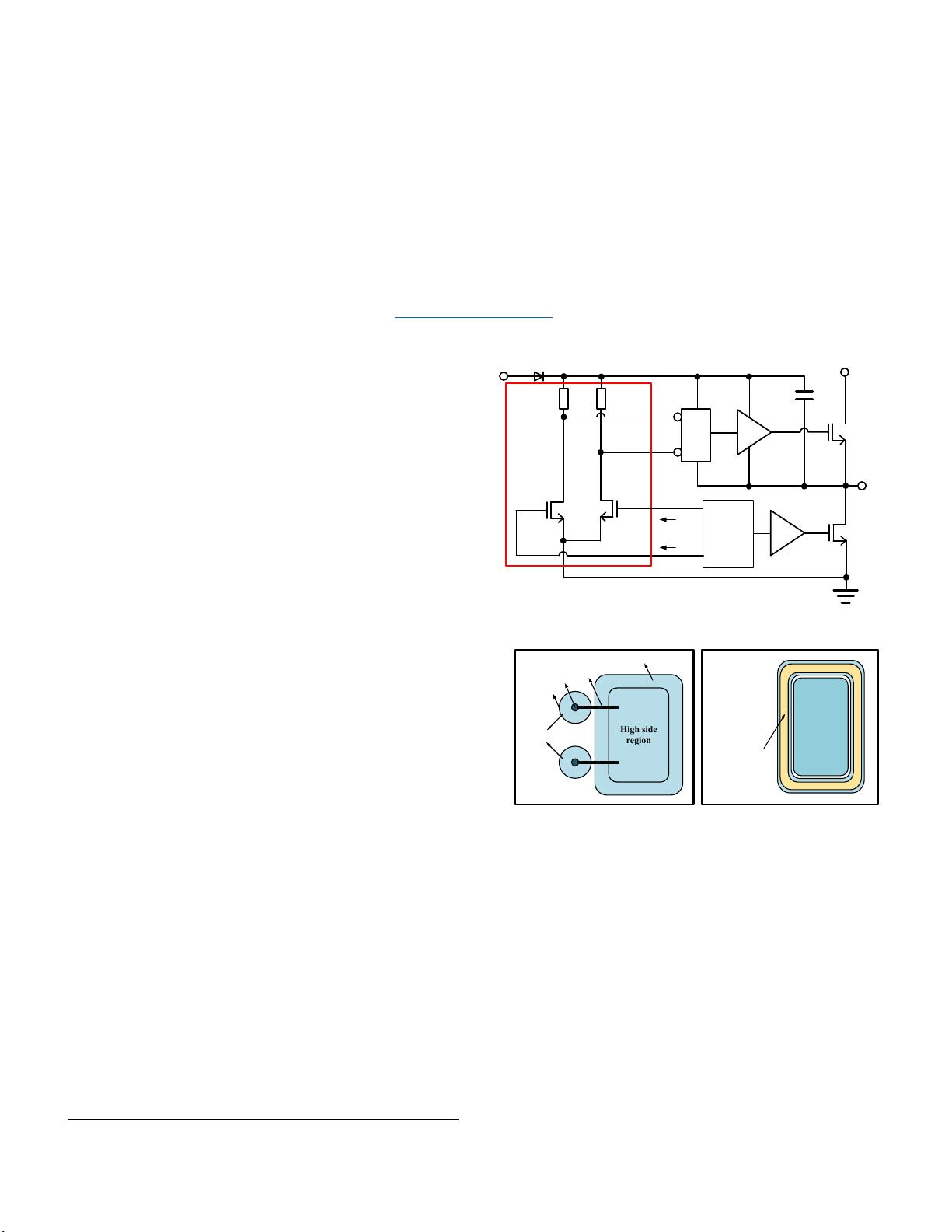
electronic ballast, and etc. [1]. Fig. 1 shows the schematic of
typical HVIC. Generally speaking, HVIC contains a low-side
region and a high–side region which are isolated by High
Voltage Edge Termination (HVET) region. The low-side
control circuit produces two kinds of signals, one of which is
used to control low-side power switch M
L
, and the other one is
used to control high-side power switch M
H
. To control the
high-side devices from low-side, a high-voltage level-shifter is
necessary [2].
The red wire-frame of Fig. 1 presents the typical high-
voltage level-shifter which contains two LDMOSTs (M
1
, M
2
)
and two resistors (R
1
, R
2
). M
1
and M
2
are driven by narrow
pulses V
in1
and V
in2
that generated from low-side control circuit.
V
out1
and V
out2
are the drain voltage of M
1
and M
2
, and they are
synchronous with V
in1
and V
in2
respectively. Fig. 2 (a) shows
the layout diagram of typical HVIC. Since the drift region
length of LDMOS must be wide enough to support high
blocking voltage, the LDMOS for level-shifting occupies a
large area. Meanwhile, the High Voltage Interconnection
(HVI) between the LDMOS and the HVET region in some
cases brings an electric field concentration and restricts the
maximum voltage of HVIC [3]. Some papers proposed
different kinds of structures to avoid the problem [4-10]. For
solving the problem, this paper proposes a novel level-shifter
which mainly consists of one LDMOS and one P-i-N diode
integrated in the HVET region, as shown in Fig. 2 (b).
Compared with Fig. 2 (a), the area of the level-shifter is saved,
and the interconnection-induced pre-breakdown is avoided.
Simulation results verify the required level-shifting function of
the integrated structure.
LDMOS
M
2
R
1
R
S
Q
DrvH
DrvL
V
CC
M
L
V
BUS
GND
to load
M
H
V
out1
V
out2
D
boot
C
boot
R
2
Low
side
control
circuits
V
boot
High
voltage
level-
shifter
M
1
LDMOS
V
tub
V
in2
V
in1
Fig. 1. Schematic of typical HVIC.
High side
region
Low side
region
HVET region
(Nch-LDMOS
&P-i-N Diode)
High side
region
HVET region
LDMOS (M
1,
M
2
)
Low side
region
Drain
Source
HVI
(a)
(b)
Fig. 2. Layout diagram of (a) typical HVIC and (b) HVIC that integrates
LDMOS and P-i-N diode on the HVET region.
II. DISCUSSION ON THE PROPOSED LEVEL-SHIFTER
The schematic of HVIC that contains the proposed level-
shifter is shown in Fig. 3. V
tub
is the tub voltage of the HVIC,
and its voltage value is determined according to the states of
power switches M
H
and M
L
. When M
H
is on and M
L
is off, V
tub
≈ V
BUS
. When M
H
is off and M
L
is on, V
tub
≈ V
GND
. V
boot
is the
supplied voltage in the high-side region, and its voltage value
always follows V
tub
because of the bootstrap diode D
boot
and
capacitor C
boot
.
Project supported by the National Science Foundation of China fo
Young Scholars (Grant No. 61504021) and the State Key Program of National
atural Science of China (Grant No. 51237001).
Proc. of the 2017 IEEE Region 10 Conference (TENCON), Malaysia, November 5-8, 2017
978-1-5090-1134-6/17/$31.00 ©2017 IEEE 2683


