OPA347, 2347, 4347
8
SBOS167D
www.ti.com
COMMON-MODE REJECTION
The CMRR for the OPA347 is specified in several ways so
the best match for a given application may be used. First, the
CMRR of the device in the common-mode range below the
transition region (V
CM
< (V+) – 1.7V) is given. This specifica-
tion is the best indicator of the capability of the device when
the application requires use of one of the differential input
pairs. Second, the CMRR at V
S
= 5.5V over the entire
common-mode range is specified.
INPUT VOLTAGE
The input common-mode range extends from (V–) – 0.2V to
(V+) + 0.2V. For normal operation, inputs should be limited
to this range. The absolute maximum input voltage is 500mV
beyond the supplies. Inputs greater than the input
common-mode range but less than the maximum input
voltage, while not valid, will not cause any damage to the op
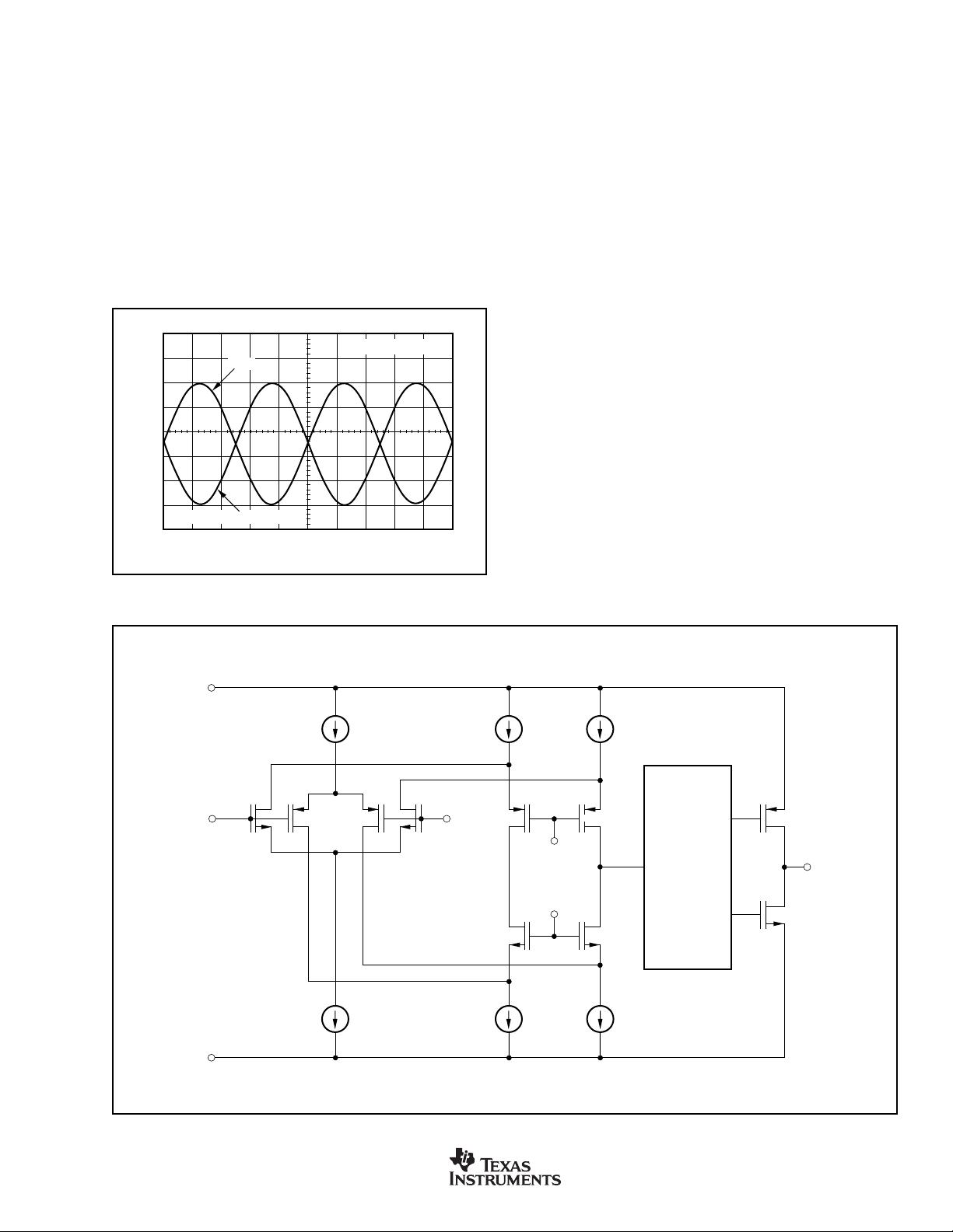
amp. Furthermore, if input current is limited the inputs may go
beyond the power supplies without phase inversion, as
shown in Figure 4, unlike some other op amps.
Normally, input currents are 0.4pA. However, large inputs
(greater than 500mV beyond the supply rails) can cause
excessive current to flow in or out of the input pins. There-
fore, as well as keeping the input voltage below the maxi-
mum rating, it is also important to limit the input current to
less than 10mA. This is easily accomplished with an input
resistor, as shown in Figure 5.
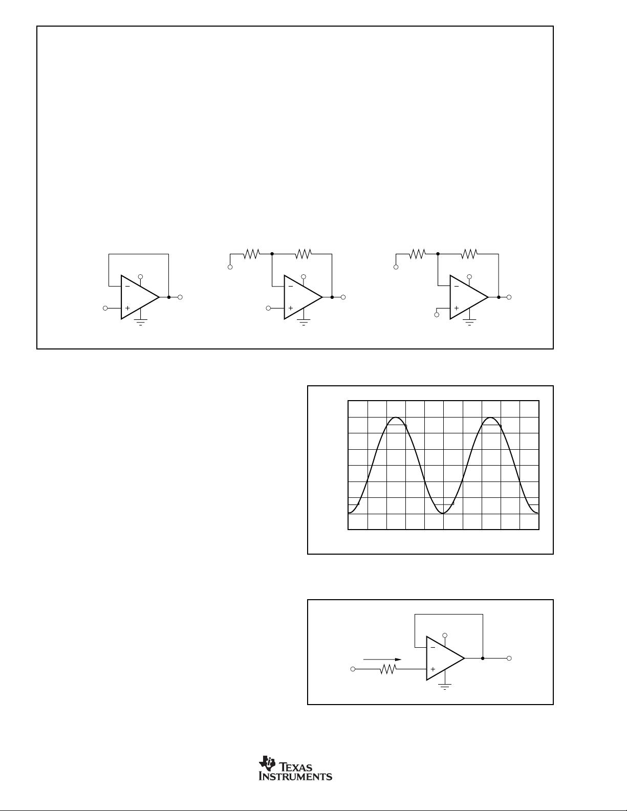
FIGURE 3. Design Optimization with Rail-to-Rail Input Op Amps.
Rail-to-rail op amps can be used in virtually any op amp
configuration. To achieve optimum performance, how-
ever, applications using these special double-input-stage
op amps may benefit from consideration of their special
behavior.
In many applications, operation remains within the com-
mon-mode range of only one differential input pair. How-
ever, some applications exercise the amplifier through the
transition region of both differential input stages. A small
discontinuity may occur in this transition. Careful selection
of the circuit configuration, signal levels, and biasing can
often avoid this transition region.
DESIGN OPTIMIZATION WITH RAIL-TO-RAIL INPUT OP AMPS
With a unity-gain buffer, for example, signals will traverse
this transition at approximately 1.3V below the V+ supply
and may exhibit a small discontinuity at this point.
The common-mode voltage of the noninverting amplifier
is equal to the input voltage. If the input signal always
remains less than the transition voltage, no discontinuity
will be created. The closed-loop gain of this configuration
can still produce a rail-to-rail output.
Inverting amplifiers have a constant common-mode volt-
age equal to V
B
. If this bias voltage is constant, no
discontinuity will be created. The bias voltage can gener-
ally be chosen to avoid the transition region.
FIGURE 4. OPA347—No Phase Inversion with Inputs Greater
than the Power-Supply Voltage.
V
O
V
IN
V
B
V+
Noninverting Amplifier
V
CM
= V
IN
V
O
V
B
V
IN
V+
Inverting Amplifier
V
CM
= V
B
V
O
V
IN
V+
Unity-Gain Buffer
V
CM
= V
IN
= V
O
FIGURE 5. Input Current Protection for Voltages Exceeding
the Supply Voltage.
5kΩ
OPA347
10mA max
+5V
V
IN
V
OUT
I
OVERLOAD
5.5V
0V
–0.5V
200µs/div


