stm32f429标准库下载
时间: 2023-08-05 09:00:32 浏览: 64
要下载STM32F429的标准库,可以按照以下步骤进行:
1. 首先,访问STMicroelectronics官方网站(https://www.st.com)。
2. 在网站的搜索栏中输入“STM32F429标准库”或者“STM32CubeF4”来查找相关资源。
3. 确保选择的是最新版本的标准库,并且与您使用的STM32F429型号兼容。
4. 找到适用于您的开发环境的下载链接,可以选择支持的操作系统(如Windows、Linux等)。
5. 单击下载链接,您可能需要创建一个免费的ST账号来访问下载页面。
6. 下载并解压缩标准库文件。该文件通常以压缩格式(如zip)提供。
7. 在解压缩后的文件夹中找到相关的文档和源代码文件,这些文件中包含了您需要使用的标准库函数和驱动程序。
8. 将这些文件添加到您的工程中。具体的添加方式可能因您使用的开发环境而有所不同,通常可以通过将文件复制到您的工程目录中或者在开发环境的项目设置中添加文件。
9. 确保正确配置您的开发环境以使用标准库。这可能包括设置适当的编译选项、链接到标准库的库文件等。
10. 最后,编译和下载您的代码到STM32F429开发板上,以验证标准库的功能和操作是否正确。
需要注意的是,以上步骤只是一个大致的指导,实际下载和使用标准库时可能会有一些细微的差异和特殊要求,具体可以参考官方提供的文档和示例代码。另外,您还可以寻找并加入STM32F429的开发者社区,以获取更多相关的支持和资源。
相关问题
stm32f429标准库例程
STM32F429标准库例程是专为STM32F429系列微控制器设计的一系列示例程序。这些例程提供了基本的应用程序框架和代码,帮助开发人员快速入门并理解如何使用STM32F429的功能和特性。
这些标准库例程涵盖了各种不同的功能,包括引脚控制、定时器、中断处理、串口通信、SPI和I2C总线通信、ADC和DAC输入输出等。通过学习和使用这些例程,开发人员可以了解系统的工作原理,掌握STM32F429的各种功能模块的使用方法。
使用这些例程的步骤通常包括以下几个步骤:
首先,开发人员需要创建一个新的项目,并选择适用于STM32F429的标准库。
其次,可以通过打开例程文件夹并选择感兴趣的例程来查找和复制所需代码。例如,要使用UART通信,开发人员可以复制相应的UART例程代码。
然后,将复制的代码粘贴到新项目的相应源文件中,并根据需要进行适当的修改和配置。例如,配置引脚、设置定时器参数等。
接下来,编译和下载代码到STM32F429微控制器。使用开发板或调试器进行调试和测试。
最后,在测试过程中发现问题时,可以参考代码和手册进行排查和解决。此外,还可以在STM32官方论坛和社区中搜索和讨论相关问题。
总之,STM32F429标准库例程是一个很好的学习和使用STM32F429微控制器的资源。通过掌握这些例程,开发人员可以更轻松地开发出各种应用程序,并充分发挥STM32F429的功能和性能。
stm32f429标准库sdram例程
以下是基于STM32F429标准库的SDRAM例程:
```c
#include "stm32f4xx.h"
#include "stm32f429i_discovery_sdram.h"
#define SDRAM_TIMEOUT ((uint32_t)0xFFFF)
int main(void)
{
/* Enable GPIOC, GPIOD, GPIOE, GPIOF, GPIOG and AFIO clocks */
RCC_AHB1PeriphClockCmd(RCC_AHB1Periph_GPIOC | RCC_AHB1Periph_GPIOD | RCC_AHB1Periph_GPIOE | RCC_AHB1Periph_GPIOF | RCC_AHB1Periph_GPIOG, ENABLE);
RCC_APB2PeriphClockCmd(RCC_APB2Periph_SYSCFG, ENABLE);
/* Initialize SDRAM */
SDRAM_Init();
/* Write data to SDRAM */
SDRAM_WriteData(0xC0000000, 0x12345678);
/* Read data from SDRAM */
uint32_t data = SDRAM_ReadData(0xC0000000);
while (1);
}
void SDRAM_Init(void)
{
GPIO_InitTypeDef GPIO_InitStructure;
/* Enable FMC clock */
RCC_AHB3PeriphClockCmd(RCC_AHB3Periph_FMC, ENABLE);
/* Configure SDNE1 and SDCKE1 pins */
GPIO_InitStructure.GPIO_Pin = GPIO_Pin_5 | GPIO_Pin_6;
GPIO_InitStructure.GPIO_Mode = GPIO_Mode_AF;
GPIO_InitStructure.GPIO_OType = GPIO_OType_PP;
GPIO_InitStructure.GPIO_PuPd = GPIO_PuPd_NOPULL;
GPIO_InitStructure.GPIO_Speed = GPIO_Speed_100MHz;
GPIO_Init(GPIOC, &GPIO_InitStructure);
GPIO_PinAFConfig(GPIOC, GPIO_PinSource5, GPIO_AF_FMC);
GPIO_PinAFConfig(GPIOC, GPIO_PinSource6, GPIO_AF_FMC);
/* Configure A0-A3 pins */
GPIO_InitStructure.GPIO_Pin = GPIO_Pin_0 | GPIO_Pin_1 | GPIO_Pin_2 | GPIO_Pin_3;
GPIO_InitStructure.GPIO_Mode = GPIO_Mode_AF;
GPIO_InitStructure.GPIO_OType = GPIO_OType_PP;
GPIO_InitStructure.GPIO_PuPd = GPIO_PuPd_NOPULL;
GPIO_InitStructure.GPIO_Speed = GPIO_Speed_100MHz;
GPIO_Init(GPIOD, &GPIO_InitStructure);
GPIO_PinAFConfig(GPIOD, GPIO_PinSource0, GPIO_AF_FMC);
GPIO_PinAFConfig(GPIOD, GPIO_PinSource1, GPIO_AF_FMC);
GPIO_PinAFConfig(GPIOD, GPIO_PinSource2, GPIO_AF_FMC);
GPIO_PinAFConfig(GPIOD, GPIO_PinSource3, GPIO_AF_FMC);
/* Configure D0-D3 pins */
GPIO_InitStructure.GPIO_Pin = GPIO_Pin_14 | GPIO_Pin_15 | GPIO_Pin_0 | GPIO_Pin_1;
GPIO_InitStructure.GPIO_Mode = GPIO_Mode_AF;
GPIO_InitStructure.GPIO_OType = GPIO_OType_PP;
GPIO_InitStructure.GPIO_PuPd = GPIO_PuPd_NOPULL;
GPIO_InitStructure.GPIO_Speed = GPIO_Speed_100MHz;
GPIO_Init(GPIOE, &GPIO_InitStructure);
GPIO_PinAFConfig(GPIOE, GPIO_PinSource14, GPIO_AF_FMC);
GPIO_PinAFConfig(GPIOE, GPIO_PinSource15, GPIO_AF_FMC);
GPIO_PinAFConfig(GPIOE, GPIO_PinSource0, GPIO_AF_FMC);
GPIO_PinAFConfig(GPIOE, GPIO_PinSource1, GPIO_AF_FMC);
/* Configure D4-D11 pins */
GPIO_InitStructure.GPIO_Pin = GPIO_Pin_7 | GPIO_Pin_8 | GPIO_Pin_9 | GPIO_Pin_10 | GPIO_Pin_11 | GPIO_Pin_12 | GPIO_Pin_13 | GPIO_Pin_14;
GPIO_InitStructure.GPIO_Mode = GPIO_Mode_AF;
GPIO_InitStructure.GPIO_OType = GPIO_OType_PP;
GPIO_InitStructure.GPIO_PuPd = GPIO_PuPd_NOPULL;
GPIO_InitStructure.GPIO_Speed = GPIO_Speed_100MHz;
GPIO_Init(GPIOF, &GPIO_InitStructure);
GPIO_PinAFConfig(GPIOF, GPIO_PinSource7, GPIO_AF_FMC);
GPIO_PinAFConfig(GPIOF, GPIO_PinSource8, GPIO_AF_FMC);
GPIO_PinAFConfig(GPIOF, GPIO_PinSource9, GPIO_AF_FMC);
GPIO_PinAFConfig(GPIOF, GPIO_PinSource10, GPIO_AF_FMC);
GPIO_PinAFConfig(GPIOF, GPIO_PinSource11, GPIO_AF_FMC);
GPIO_PinAFConfig(GPIOF, GPIO_PinSource12, GPIO_AF_FMC);
GPIO_PinAFConfig(GPIOF, GPIO_PinSource13, GPIO_AF_FMC);
GPIO_PinAFConfig(GPIOF, GPIO_PinSource14, GPIO_AF_FMC);
/* Configure D12-D15 pins */
GPIO_InitStructure.GPIO_Pin = GPIO_Pin_0 | GPIO_Pin_1 | GPIO_Pin_2 | GPIO_Pin_3;
GPIO_InitStructure.GPIO_Mode = GPIO_Mode_AF;
GPIO_InitStructure.GPIO_OType = GPIO_OType_PP;
GPIO_InitStructure.GPIO_PuPd = GPIO_PuPd_NOPULL;
GPIO_InitStructure.GPIO_Speed = GPIO_Speed_100MHz;
GPIO_Init(GPIOG, &GPIO_InitStructure);
GPIO_PinAFConfig(GPIOG, GPIO_PinSource0, GPIO_AF_FMC);
GPIO_PinAFConfig(GPIOG, GPIO_PinSource1, GPIO_AF_FMC);
GPIO_PinAFConfig(GPIOG, GPIO_PinSource2, GPIO_AF_FMC);
GPIO_PinAFConfig(GPIOG, GPIO_PinSource3, GPIO_AF_FMC);
/* SDRAM initialization sequence */
FMC_SDRAMTimingInitTypeDef SDRAM_Timing_InitStructure;
FMC_SDRAMInitTypeDef SDRAM_InitStructure;
SDRAM_Timing_InitStructure.FMC_LoadToActiveDelay = 2;
SDRAM_Timing_InitStructure.FMC_ExitSelfRefreshDelay = 7;
SDRAM_Timing_InitStructure.FMC_SelfRefreshTime = 4;
SDRAM_Timing_InitStructure.FMC_RowCycleDelay = 7;
SDRAM_Timing_InitStructure.FMC_WriteRecoveryTime = 2;
SDRAM_Timing_InitStructure.FMC_RPDelay = 2;
SDRAM_Timing_InitStructure.FMC_RCDDelay = 2;
SDRAM_InitStructure.FMC_Bank = FMC_Bank2_SDRAM;
SDRAM_InitStructure.FMC_ColumnBitsNumber = FMC_ColumnBits_Number_8b;
SDRAM_InitStructure.FMC_RowBitsNumber = FMC_RowBits_Number_12b;
SDRAM_InitStructure.FMC_SDMemoryDataWidth = FMC_SDMemory_Width_16b;
SDRAM_InitStructure.FMC_InternalBankNumber = FMC_InternalBank_Number_4;
SDRAM_InitStructure.FMC_CASLatency = FMC_CAS_Latency_2;
SDRAM_InitStructure.FMC_WriteProtection = FMC_Write_Protection_Disable;
SDRAM_InitStructure.FMC_SDClockPeriod = FMC_SDClock_Period_2;
SDRAM_InitStructure.FMC_ReadBurst = FMC_Read_Burst_Disable;
SDRAM_InitStructure.FMC_ReadPipeDelay = FMC_ReadPipe_Delay_1;
SDRAM_InitStructure.FMC_SDRAMTimingStruct = &SDRAM_Timing_InitStructure;
FMC_SDRAMInit(&SDRAM_InitStructure);
/* SDRAM bank enable */
FMC_SDRAMCmdConfigTypeDef SDRAM_Cmd_InitStructure;
SDRAM_Cmd_InitStructure.FMC_CommandMode = FMC_Command_Mode_CLK_Enabled;
SDRAM_Cmd_InitStructure.FMC_CommandTarget = FMC_Command_Target_bank2;
SDRAM_Cmd_InitStructure.FMC_AutoRefreshNumber = 1;
SDRAM_Cmd_InitStructure.FMC_ModeRegisterDefinition = 0;
FMC_SDRAMCmdConfig(&SDRAM_Cmd_InitStructure);
/* Wait for SDRAM initialization */
uint32_t timeout = SDRAM_TIMEOUT;
while (FMC_GetFlagStatus(FMC_Bank2_SDRAM, FMC_FLAG_BUSY) != RESET)
{
if (timeout-- == 0)
{
/* SDRAM initialization error */
while (1);
}
}
}
void SDRAM_WriteData(uint32_t addr, uint32_t data)
{
/* Write data to SDRAM */
*(uint32_t *)addr = data;
}
uint32_t SDRAM_ReadData(uint32_t addr)
{
/* Read data from SDRAM */
return *(uint32_t *)addr;
}
```
这个例程用到了SDRAM外设,需要连接到MCU的外部引脚。具体的SDRAM引脚分配可以在STM32F429I Discovery板手册中找到。在本例程中,SDRAM连接到了MCU的Bank2,使用16位数据总线,12位行地址和8位列地址。在初始化SDRAM时,需要设置SDRAM的时序参数。在写入和读取数据时,需要将SDRAM地址转换为指针,并使用指针进行数据传输。
相关推荐
最新推荐
STM32F103固件函数库用户手册(中文)
STM32F103固件函数库是针对基于ARM微控制器的32位STM32F101xx和STM32F103xx系列设计的一个全面的软件包,旨在简化用户对这些微控制器外设的使用。这个库包含了一系列的程序、数据结构和宏,覆盖了所有外设的功能特性...
BSC绩效考核指标汇总 (2).docx
BSC(Balanced Scorecard,平衡计分卡)是一种战略绩效管理系统,它将企业的绩效评估从传统的财务维度扩展到非财务领域,以提供更全面、深入的业绩衡量。在提供的文档中,BSC绩效考核指标主要分为两大类:财务类和客户类。
1. 财务类指标:
- 部门费用的实际与预算比较:如项目研究开发费用、课题费用、招聘费用、培训费用和新产品研发费用,均通过实际支出与计划预算的百分比来衡量,这反映了部门在成本控制上的效率。
- 经营利润指标:如承保利润、赔付率和理赔统计,这些涉及保险公司的核心盈利能力和风险管理水平。
- 人力成本和保费收益:如人力成本与计划的比例,以及标准保费、附加佣金、续期推动费用等与预算的对比,评估业务运营和盈利能力。
- 财务效率:包括管理费用、销售费用和投资回报率,如净投资收益率、销售目标达成率等,反映公司的财务健康状况和经营效率。
2. 客户类指标:
- 客户满意度:通过包装水平客户满意度调研,了解产品和服务的质量和客户体验。
- 市场表现:通过市场销售月报和市场份额,衡量公司在市场中的竞争地位和销售业绩。
- 服务指标:如新契约标保完成度、续保率和出租率,体现客户服务质量和客户忠诚度。
- 品牌和市场知名度:通过问卷调查、公众媒体反馈和总公司级评价来评估品牌影响力和市场认知度。
BSC绩效考核指标旨在确保企业的战略目标与财务和非财务目标的平衡,通过量化这些关键指标,帮助管理层做出决策,优化资源配置,并驱动组织的整体业绩提升。同时,这份指标汇总文档强调了财务稳健性和客户满意度的重要性,体现了现代企业对多维度绩效管理的重视。
管理建模和仿真的文件
管理Boualem Benatallah引用此版本:布阿利姆·贝纳塔拉。管理建模和仿真。约瑟夫-傅立叶大学-格勒诺布尔第一大学,1996年。法语。NNT:电话:00345357HAL ID:电话:00345357https://theses.hal.science/tel-003453572008年12月9日提交HAL是一个多学科的开放存取档案馆,用于存放和传播科学研究论文,无论它们是否被公开。论文可以来自法国或国外的教学和研究机构,也可以来自公共或私人研究中心。L’archive ouverte pluridisciplinaire
【进阶】Flask中的会话与用户管理
# 2.1 用户注册和登录
### 2.1.1 用户注册表单的设计和验证
用户注册表单是用户创建帐户的第一步,因此至关重要。它应该简单易用,同时收集必要的用户信息。
* **字段设计:**表单应包含必要的字段,如用户名、电子邮件和密码。
* **验证:**表单应验证字段的格式和有效性,例如电子邮件地址的格式和密码的强度。
* **错误处理:**表单应优雅地处理验证错误,并提供清晰的错误消
卷积神经网络实现手势识别程序
卷积神经网络(Convolutional Neural Network, CNN)在手势识别中是一种非常有效的机器学习模型。CNN特别适用于处理图像数据,因为它能够自动提取和学习局部特征,这对于像手势这样的空间模式识别非常重要。以下是使用CNN实现手势识别的基本步骤:
1. **输入数据准备**:首先,你需要收集或获取一组带有标签的手势图像,作为训练和测试数据集。
2. **数据预处理**:对图像进行标准化、裁剪、大小调整等操作,以便于网络输入。
3. **卷积层(Convolutional Layer)**:这是CNN的核心部分,通过一系列可学习的滤波器(卷积核)对输入图像进行卷积,以
BSC资料.pdf
"BSC资料.pdf"
战略地图是一种战略管理工具,它帮助企业将战略目标可视化,确保所有部门和员工的工作都与公司的整体战略方向保持一致。战略地图的核心内容包括四个相互关联的视角:财务、客户、内部流程和学习与成长。
1. **财务视角**:这是战略地图的最终目标,通常表现为股东价值的提升。例如,股东期望五年后的销售收入达到五亿元,而目前只有一亿元,那么四亿元的差距就是企业的总体目标。
2. **客户视角**:为了实现财务目标,需要明确客户价值主张。企业可以通过提供最低总成本、产品创新、全面解决方案或系统锁定等方式吸引和保留客户,以实现销售额的增长。
3. **内部流程视角**:确定关键流程以支持客户价值主张和财务目标的实现。主要流程可能包括运营管理、客户管理、创新和社会责任等,每个流程都需要有明确的短期、中期和长期目标。
4. **学习与成长视角**:评估和提升企业的人力资本、信息资本和组织资本,确保这些无形资产能够支持内部流程的优化和战略目标的达成。
绘制战略地图的六个步骤:
1. **确定股东价值差距**:识别与股东期望之间的差距。
2. **调整客户价值主张**:分析客户并调整策略以满足他们的需求。
3. **设定价值提升时间表**:规划各阶段的目标以逐步缩小差距。
4. **确定战略主题**:识别关键内部流程并设定目标。
5. **提升战略准备度**:评估并提升无形资产的战略准备度。
6. **制定行动方案**:根据战略地图制定具体行动计划,分配资源和预算。
战略地图的有效性主要取决于两个要素:
1. **KPI的数量及分布比例**:一个有效的战略地图通常包含20个左右的指标,且在四个视角之间有均衡的分布,如财务20%,客户20%,内部流程40%。
2. **KPI的性质比例**:指标应涵盖财务、客户、内部流程和学习与成长等各个方面,以全面反映组织的绩效。
战略地图不仅帮助管理层清晰传达战略意图,也使员工能更好地理解自己的工作如何对公司整体目标产生贡献,从而提高执行力和组织协同性。
"互动学习:行动中的多样性与论文攻读经历"
多样性她- 事实上SCI NCES你的时间表ECOLEDO C Tora SC和NCESPOUR l’Ingén学习互动,互动学习以行动为中心的强化学习学会互动,互动学习,以行动为中心的强化学习计算机科学博士论文于2021年9月28日在Villeneuve d'Asq公开支持马修·瑟林评审团主席法布里斯·勒菲弗尔阿维尼翁大学教授论文指导奥利维尔·皮耶昆谷歌研究教授:智囊团论文联合主任菲利普·普雷教授,大学。里尔/CRISTAL/因里亚报告员奥利维耶·西格德索邦大学报告员卢多维奇·德诺耶教授,Facebook /索邦大学审查员越南圣迈IMT Atlantic高级讲师邀请弗洛里安·斯特鲁布博士,Deepmind对于那些及时看到自己错误的人...3谢谢你首先,我要感谢我的两位博士生导师Olivier和Philippe。奥利维尔,"站在巨人的肩膀上"这句话对你来说完全有意义了。从科学上讲,你知道在这篇论文的(许多)错误中,你是我可以依
【进阶】Flask中的请求处理
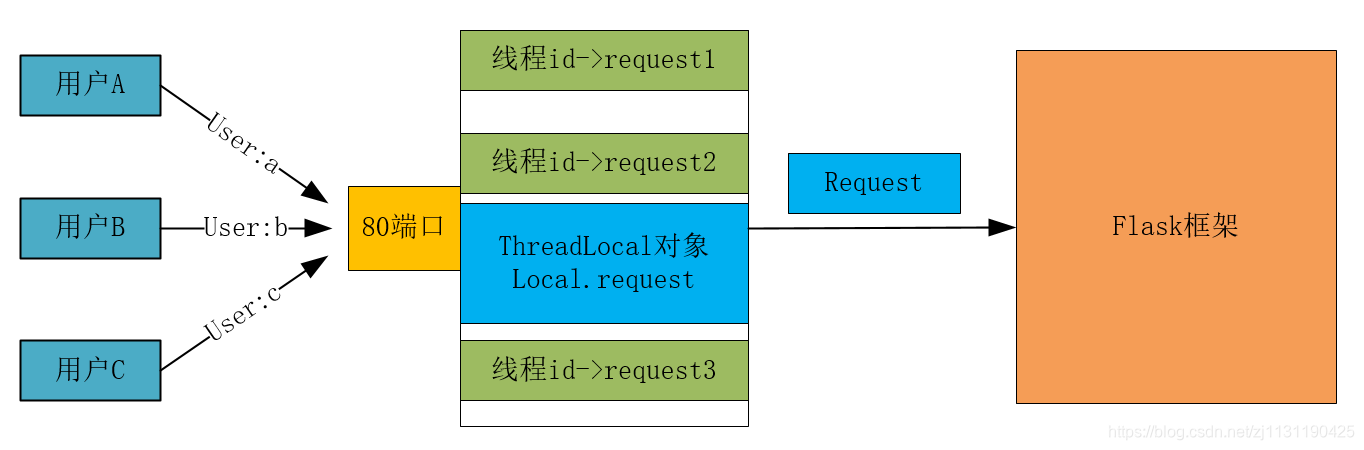
# 1. Flask请求处理概述**
Flask是一个轻量级的Web框架,它提供了一个简洁且灵活的接口来处理HTTP请求。在Flask中,请求处理是一个核心概念,它允许
transformer模型对话
Transformer模型是一种基于自注意力机制的深度学习架构,最初由Google团队在2017年的论文《Attention is All You Need》中提出,主要用于自然语言处理任务,如机器翻译和文本生成。Transformer完全摒弃了传统的循环神经网络(RNN)和卷积神经网络(CNN),转而采用全连接的方式处理序列数据,这使得它能够并行计算,极大地提高了训练速度。
在对话系统中,Transformer模型通过编码器-解码器结构工作。编码器将输入序列转化为固定长度的上下文向量,而解码器则根据这些向量逐步生成响应,每一步都通过自注意力机制关注到输入序列的所有部分,这使得模型能够捕捉到
BSC绩效考核指标汇总 (3).pdf
BSC(Balanced Scorecard,平衡计分卡)是一种企业绩效管理系统,它将公司的战略目标分解为四个维度:财务、客户、内部流程和学习与成长。在这个文档中,我们看到的是针对特定行业(可能是保险或保险经纪)的BSC绩效考核指标汇总,专注于财务类和非财务类的关键绩效指标(KPIs)。
财务类指标:
1. 部门费用预算达成率:衡量实际支出与计划费用之间的对比,通过公式 (实际部门费用/计划费用)*100% 来计算,数据来源于部门的预算和实际支出记录。
2. 项目研究开发费用预算达成率:同样用于评估研发项目的资金管理,公式为 (实际项目研究开发费用/计划费用)*100%。
3. 课题费用预算达成率、招聘费用预算达成率、培训费用预算达成率 和 新产品研究开发费用预算达成率:这些都是人力资源相关开支的预算执行情况,涉及到费用的实际花费与计划金额的比例。
4. 承保利润:衡量保险公司盈利能力的重要指标,包括赔付率和寿险各险种的死差损益(实际死亡率与预期死亡率的差异)。
5. 赔付率:反映保险公司的赔付情况,是业务健康度的一个关键指标。
6. 内嵌价值的增加:代表了保单的价值增长,反映了公司长期盈利能力。
7. 人力成本总额控制率:通过比较实际人力成本与计划成本来评估人力成本的有效管理。
8. 标准保费达成率:衡量公司的销售业绩,即实际收取保费与目标保费的比率。
9. 其他费用比率,如附加佣金、续期推动费用、业务推动费用等,用来评估营销费用的效率。
非财务类指标:
1. 销售目标达成率:衡量销售团队完成预定目标的程度,通过实际销售额与计划销售额的比率计算。
2. 理赔率:体现客户服务质量和效率,涉及保险公司处理理赔请求的速度和成功率。
3. 产品/服务销售收入达成率:衡量产品或服务的实际销售效果,反映市场响应和客户满意度。
这些指标集合在一起,提供了全面的视角来评估公司的经营效率、财务表现以及战略执行情况。通过定期跟踪和分析这些数据,企业可以持续优化策略,提升业绩,确保与整体战略目标的一致性。每个指标的数据来源通常来自于相关部门的预算和实际操作记录,确保信息的准确性。