module chaoqian(C,G,P,Ci); output[4:1] C; input[3:0] G,P; input Ci; wire[4:1] C; wire[3:0] G,P; assign C[1]=G[0]|(P[0]&Ci); assign C[2]=G[1]|(P[1]&G[0])|(P[1]&P[0]&Ci); assign C[3]=G[2]|(P[2]&G[1])|(P[2]&P[1]&G[0])|(P[2]&P[1]&P[0]&Ci); assign C[4]=G[3]|(P[3]&G[2])|(P[3]&P[2]&G[1])|(P[3]&P[2]&P[1]&G[0])|(P[3]&P[2]&P[1]&P[0]&Ci); endmodule每一行代码的意思
时间: 2023-10-03 08:09:24 浏览: 43
这段代码是一个 Verilog HDL 的模块定义,用于描述一个 4 位超前进位加法器(carry lookahead adder),其具体功能是将两个 4 位二进制数相加,并产生一个 4 位二进制和。
具体每一行代码的意思如下:
- 第 1 行:定义一个名为 chaoqian 的模块,它有三个输入 G、P、Ci 和一个 4 位输出 C。
- 第 2~3 行:声明输出信号 C 和输入信号 G、P、Ci。
- 第 4~7 行:使用 assign 语句来为输出信号 C 的每个位分别赋值。其中,C[1] 的值为 G[0] 或 (P[0] and Ci),C[2] 的值为 G[1] 或 (P[1] and G[0]) 或 (P[1] and P[0] and Ci),C[3] 的值为 G[2] 或 (P[2] and G[1]) 或 (P[2] and P[1] and G[0]) 或 (P[2] and P[1] and P[0] and Ci),C[4] 的值为 G[3] 或 (P[3] and G[2]) 或 (P[3] and P[2] and G[1]) 或 (P[3] and P[2] and P[1] and G[0]) 或 (P[3] and P[2] and P[1] and P[0] and Ci)。
其中,G 表示每个数位相加时是否需要进位的控制信号(1 表示需要进位,0 表示不需要进位),P 表示每个数位相加时的输入信号(0 或 1),Ci 表示全加器的输入进位信号,C 表示相加的结果(0 或 1)。超前进位加法器是一种通过预先计算进位信号,以加速加法器的运算速度的技术。
相关推荐
最新推荐
JAVA图书馆书库管理系统设计(论文+源代码).zip
JAVA图书馆书库管理系统设计(论文+源代码)
unity直接从excel中读取数据,暂存数据格式为dic<string,Object>
unity直接从excel中读取数据,暂存数据格式为dic<string,Object>,string为sheet表名,Object为List<表中对应的实体类>,可以自行获取数据进行转换。核心方法为ImportExcelFiles,参数有
string[]<param name="filePaths">多个excel文件路径</param>
Assembly<param name="assembly">程序集</param>
string<param name="namespacePrefix">命名空间</param>
Dictionary<string, string><param name="sheetNameShiftDic">映射表</param>
基于SSM++jsp的在线医疗服务系统(免费提供全套java开源毕业设计源码+数据库+开题报告+论文+ppt+使用说明)
网络技术和计算机技术发展至今,已经拥有了深厚的理论基础,并在现实中进行了充分运用,尤其是基于计算机运行的软件更是受到各界的关注。加上现在人们已经步入信息时代,所以对于信息的宣传和管理就很关键。因此医疗服务信息的管理计算机化,系统化是必要的。设计开发在线医疗服务系统不仅会节约人力和管理成本,还会安全保存庞大的数据量,对于医疗服务信息的维护和检索也不需要花费很多时间,非常的便利。
在线医疗服务系统是在MySQL中建立数据表保存信息,运用SSM框架和Java语言编写。并按照软件设计开发流程进行设计实现。系统具备友好性且功能完善。管理员管理医生,药品,预约挂号,购买订单以及用户病例等信息。医生管理坐诊信息,审核预约挂号,管理用户病例。用户查看医生坐诊,对医生预约挂号,在线购买药品。
在线医疗服务系统在让医疗服务信息规范化的同时,也能及时通过数据输入的有效性规则检测出错误数据,让数据的录入达到准确性的目的,进而提升在线医疗服务系统提供的数据的可靠性,让系统数据的错误率降至最低。
关键词:在线医疗服务系统;MySQL;SSM框架
智能制造与数字化工厂.pptx
智能制造与数字化工厂.pptx
经典算法Matlab仿真设计:傅里叶变换、滤波器、FFT详解与实现
经典算法Matlab仿真设计:傅里叶变换、滤波器、FFT详解与实现
BSC关键绩效财务与客户指标详解
BSC(Balanced Scorecard,平衡计分卡)是一种战略绩效管理系统,它将企业的绩效评估从传统的财务维度扩展到非财务领域,以提供更全面、深入的业绩衡量。在提供的文档中,BSC绩效考核指标主要分为两大类:财务类和客户类。
1. 财务类指标:
- 部门费用的实际与预算比较:如项目研究开发费用、课题费用、招聘费用、培训费用和新产品研发费用,均通过实际支出与计划预算的百分比来衡量,这反映了部门在成本控制上的效率。
- 经营利润指标:如承保利润、赔付率和理赔统计,这些涉及保险公司的核心盈利能力和风险管理水平。
- 人力成本和保费收益:如人力成本与计划的比例,以及标准保费、附加佣金、续期推动费用等与预算的对比,评估业务运营和盈利能力。
- 财务效率:包括管理费用、销售费用和投资回报率,如净投资收益率、销售目标达成率等,反映公司的财务健康状况和经营效率。
2. 客户类指标:
- 客户满意度:通过包装水平客户满意度调研,了解产品和服务的质量和客户体验。
- 市场表现:通过市场销售月报和市场份额,衡量公司在市场中的竞争地位和销售业绩。
- 服务指标:如新契约标保完成度、续保率和出租率,体现客户服务质量和客户忠诚度。
- 品牌和市场知名度:通过问卷调查、公众媒体反馈和总公司级评价来评估品牌影响力和市场认知度。
BSC绩效考核指标旨在确保企业的战略目标与财务和非财务目标的平衡,通过量化这些关键指标,帮助管理层做出决策,优化资源配置,并驱动组织的整体业绩提升。同时,这份指标汇总文档强调了财务稳健性和客户满意度的重要性,体现了现代企业对多维度绩效管理的重视。
管理建模和仿真的文件
管理Boualem Benatallah引用此版本:布阿利姆·贝纳塔拉。管理建模和仿真。约瑟夫-傅立叶大学-格勒诺布尔第一大学,1996年。法语。NNT:电话:00345357HAL ID:电话:00345357https://theses.hal.science/tel-003453572008年12月9日提交HAL是一个多学科的开放存取档案馆,用于存放和传播科学研究论文,无论它们是否被公开。论文可以来自法国或国外的教学和研究机构,也可以来自公共或私人研究中心。L’archive ouverte pluridisciplinaire
【实战演练】俄罗斯方块:实现经典的俄罗斯方块游戏,学习方块生成和行消除逻辑。
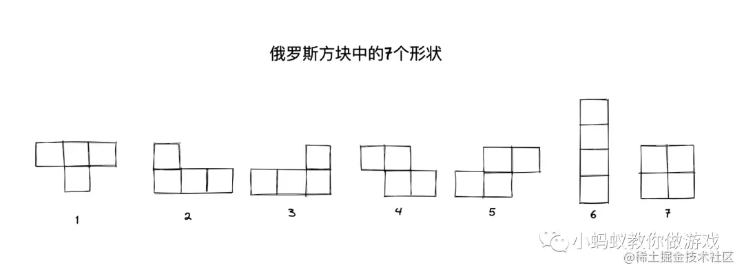
# 1. 俄罗斯方块游戏概述**
俄罗斯方块是一款经典的益智游戏,由阿列克谢·帕基特诺夫于1984年发明。游戏目标是通过控制不断下落的方块,排列成水平线,消除它们并获得分数。俄罗斯方块风靡全球,成为有史以来最受欢迎的视频游戏之一。
# 2.
卷积神经网络实现手势识别程序
卷积神经网络(Convolutional Neural Network, CNN)在手势识别中是一种非常有效的机器学习模型。CNN特别适用于处理图像数据,因为它能够自动提取和学习局部特征,这对于像手势这样的空间模式识别非常重要。以下是使用CNN实现手势识别的基本步骤:
1. **输入数据准备**:首先,你需要收集或获取一组带有标签的手势图像,作为训练和测试数据集。
2. **数据预处理**:对图像进行标准化、裁剪、大小调整等操作,以便于网络输入。
3. **卷积层(Convolutional Layer)**:这是CNN的核心部分,通过一系列可学习的滤波器(卷积核)对输入图像进行卷积,以
绘制企业战略地图:从财务到客户价值的六步法
"BSC资料.pdf"
战略地图是一种战略管理工具,它帮助企业将战略目标可视化,确保所有部门和员工的工作都与公司的整体战略方向保持一致。战略地图的核心内容包括四个相互关联的视角:财务、客户、内部流程和学习与成长。
1. **财务视角**:这是战略地图的最终目标,通常表现为股东价值的提升。例如,股东期望五年后的销售收入达到五亿元,而目前只有一亿元,那么四亿元的差距就是企业的总体目标。
2. **客户视角**:为了实现财务目标,需要明确客户价值主张。企业可以通过提供最低总成本、产品创新、全面解决方案或系统锁定等方式吸引和保留客户,以实现销售额的增长。
3. **内部流程视角**:确定关键流程以支持客户价值主张和财务目标的实现。主要流程可能包括运营管理、客户管理、创新和社会责任等,每个流程都需要有明确的短期、中期和长期目标。
4. **学习与成长视角**:评估和提升企业的人力资本、信息资本和组织资本,确保这些无形资产能够支持内部流程的优化和战略目标的达成。
绘制战略地图的六个步骤:
1. **确定股东价值差距**:识别与股东期望之间的差距。
2. **调整客户价值主张**:分析客户并调整策略以满足他们的需求。
3. **设定价值提升时间表**:规划各阶段的目标以逐步缩小差距。
4. **确定战略主题**:识别关键内部流程并设定目标。
5. **提升战略准备度**:评估并提升无形资产的战略准备度。
6. **制定行动方案**:根据战略地图制定具体行动计划,分配资源和预算。
战略地图的有效性主要取决于两个要素:
1. **KPI的数量及分布比例**:一个有效的战略地图通常包含20个左右的指标,且在四个视角之间有均衡的分布,如财务20%,客户20%,内部流程40%。
2. **KPI的性质比例**:指标应涵盖财务、客户、内部流程和学习与成长等各个方面,以全面反映组织的绩效。
战略地图不仅帮助管理层清晰传达战略意图,也使员工能更好地理解自己的工作如何对公司整体目标产生贡献,从而提高执行力和组织协同性。