how to understand "the SiGe has a higher carrier mobility compared to silicon"?
时间: 2024-05-25 11:19:24 浏览: 20
This statement means that when electric current flows through a material, the SiGe (Silicon Germanium) allows the carriers (electrons or holes) to move more easily and quickly than silicon. This higher carrier mobility in SiGe can result in faster and more efficient electronic devices.
相关问题
why the SiGe Fin can improve the performance of the transistor? especially the PMOS
The SiGe Fin can improve the performance of the transistor, especially the PMOS, due to several reasons:
1. Higher carrier mobility: SiGe has a higher carrier mobility compared to silicon, which means that electrons can move faster through the material. This results in faster switching times and higher performance.
2. Lower parasitic resistance: SiGe has a lower parasitic resistance compared to silicon, which means that there is less resistance in the material for the electrons to overcome. This results in lower power consumption and higher performance.
3. Reduced junction leakage: SiGe has a lower junction leakage compared to silicon, which means that there is less current leaking through the transistor when it is turned off. This results in higher on/off ratio and better performance.
4. Reduced short-channel effects: SiGe has a higher bandgap compared to silicon, which means that it can reduce the short-channel effects that limit the performance of PMOS transistors. This results in higher performance and better stability.
Overall, the use of SiGe Fin can improve the performance of PMOS transistors, leading to faster switching times, lower power consumption, higher on/off ratio, and better stability.
whats the crystall structure difference of SiGe fin and Si fin
The crystalline structure difference between SiGe fin and Si fin is that SiGe fin has a lattice structure that is different from pure Si. SiGe is a compound semiconductor material that is made by combining silicon (Si) and germanium (Ge) atoms. The addition of Ge atoms changes the lattice structure of the material and provides additional degrees of freedom in the design of semiconductor devices. Si fin has a pure silicon lattice structure that is commonly used in the fabrication of transistors and other electronic devices.
相关推荐
最新推荐
比较射频功率放大器的三种主要工艺技术
超CMOS工艺的优点在于能够提供与GaAs或SiGe技术相媲美甚至更好的性能,同时具有比GaAs或SiGe更优异的线性度和防静电放电(ESD)性能。 GaAs工艺是射频功率放大器的传统技术之一。GaAs的电子迁移率比作为CMOS衬底...
信氧饮吧-奶茶管理系统
奶茶管理系统
win7-2008-X86处理此操作系统不能安装/不支持.net framework 4.6.2的方法
win7-2008_X86处理此操作系统不能安装/不支持.net framework 4.6.2的方法
将现有系统升级为sp1系统即可,升级文件如下
MySQL工资管理系统
MySQL工资管理系统
机器学习课程设计-基于python实现的交通标志识别源码+文档说明+结果+数据+柱状图+模型
<项目介绍>
机器学习课设
交通标志识别
交通标志识别的作用:
有几种不同类型的交通标志,如限速,禁止进入,交通信号灯,左转或右转,儿童交叉口,不通过重型车辆等。交通标志分类是识别交通标志所属类别的过程。
在本项目中,通过构建一个深度神经网络模型,可以将图像中存在的交通标志分类为不同的类别。通过该模型,我们能够读取和理解交通标志,这对所有自动驾驶汽车来说都是一项非
-
不懂运行,下载完可以私聊问,可远程教学
该资源内项目源码是个人的毕设,代码都测试ok,都是运行成功后才上传资源,答辩评审平均分达到96分,放心下载使用!
1、该资源内项目代码都经过测试运行成功,功能ok的情况下才上传的,请放心下载使用!
2、本项目适合计算机相关专业(如计科、人工智能、通信工程、自动化、电子信息等)的在校学生、老师或者企业员工下载学习,也适合小白学习进阶,当然也可作为毕设项目、课程设计、作业、项目初期立项演示等。
3、如果基础还行,也可在此代码基础上进行修改,以实现其他功能,也可用于毕设、课设、作业等。
下载后请首先打开README.md文件(如有),仅供学习参考, 切勿用于商业用途。
--------
京瓷TASKalfa系列维修手册:安全与操作指南
"该资源是一份针对京瓷TASKalfa系列多款型号打印机的维修手册,包括TASKalfa 2020/2021/2057,TASKalfa 2220/2221,TASKalfa 2320/2321/2358,以及DP-480,DU-480,PF-480等设备。手册标注为机密,仅供授权的京瓷工程师使用,强调不得泄露内容。手册内包含了重要的安全注意事项,提醒维修人员在处理电池时要防止爆炸风险,并且应按照当地法规处理废旧电池。此外,手册还详细区分了不同型号产品的打印速度,如TASKalfa 2020/2021/2057的打印速度为20张/分钟,其他型号则分别对应不同的打印速度。手册还包括修订记录,以确保信息的最新和准确性。"
本文档详尽阐述了京瓷TASKalfa系列多功能一体机的维修指南,适用于多种型号,包括速度各异的打印设备。手册中的安全警告部分尤为重要,旨在保护维修人员、用户以及设备的安全。维修人员在操作前必须熟知这些警告,以避免潜在的危险,如不当更换电池可能导致的爆炸风险。同时,手册还强调了废旧电池的合法和安全处理方法,提醒维修人员遵守地方固体废弃物法规。
手册的结构清晰,有专门的修订记录,这表明手册会随着设备的更新和技术的改进不断得到完善。维修人员可以依靠这份手册获取最新的维修信息和操作指南,确保设备的正常运行和维护。
此外,手册中对不同型号的打印速度进行了明确的区分,这对于诊断问题和优化设备性能至关重要。例如,TASKalfa 2020/2021/2057系列的打印速度为20张/分钟,而TASKalfa 2220/2221和2320/2321/2358系列则分别具有稍快的打印速率。这些信息对于识别设备性能差异和优化工作流程非常有用。
总体而言,这份维修手册是京瓷TASKalfa系列设备维修保养的重要参考资料,不仅提供了详细的操作指导,还强调了安全性和合规性,对于授权的维修工程师来说是不可或缺的工具。
管理建模和仿真的文件
管理Boualem Benatallah引用此版本:布阿利姆·贝纳塔拉。管理建模和仿真。约瑟夫-傅立叶大学-格勒诺布尔第一大学,1996年。法语。NNT:电话:00345357HAL ID:电话:00345357https://theses.hal.science/tel-003453572008年12月9日提交HAL是一个多学科的开放存取档案馆,用于存放和传播科学研究论文,无论它们是否被公开。论文可以来自法国或国外的教学和研究机构,也可以来自公共或私人研究中心。L’archive ouverte pluridisciplinaire
【进阶】入侵检测系统简介
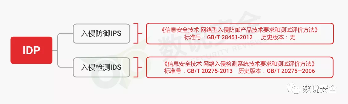
# 1. 入侵检测系统概述**
入侵检测系统(IDS)是一种网络安全工具,用于检测和预防未经授权的访问、滥用、异常或违反安全策略的行为。IDS通过监控网络流量、系统日志和系统活动来识别潜在的威胁,并向管理员发出警报。
IDS可以分为两大类:基于网络的IDS(NIDS)和基于主机的IDS(HIDS)。NIDS监控网络流量,而HIDS监控单个主机的活动。IDS通常使用签名检测、异常检测和行
轨道障碍物智能识别系统开发
轨道障碍物智能识别系统是一种结合了计算机视觉、人工智能和机器学习技术的系统,主要用于监控和管理铁路、航空或航天器的运行安全。它的主要任务是实时检测和分析轨道上的潜在障碍物,如行人、车辆、物体碎片等,以防止这些障碍物对飞行或行驶路径造成威胁。
开发这样的系统主要包括以下几个步骤:
1. **数据收集**:使用高分辨率摄像头、雷达或激光雷达等设备获取轨道周围的实时视频或数据。
2. **图像处理**:对收集到的图像进行预处理,包括去噪、增强和分割,以便更好地提取有用信息。
3. **特征提取**:利用深度学习模型(如卷积神经网络)提取障碍物的特征,如形状、颜色和运动模式。
4. **目标
小波变换在视频压缩中的应用
"多媒体通信技术视频信息压缩与处理(共17张PPT).pptx"
多媒体通信技术涉及的关键领域之一是视频信息压缩与处理,这在现代数字化社会中至关重要,尤其是在传输和存储大量视频数据时。本资料通过17张PPT详细介绍了这一主题,特别是聚焦于小波变换编码和分形编码两种新型的图像压缩技术。
4.5.1 小波变换编码是针对宽带图像数据压缩的一种高效方法。与离散余弦变换(DCT)相比,小波变换能够更好地适应具有复杂结构和高频细节的图像。DCT对于窄带图像信号效果良好,其变换系数主要集中在低频部分,但对于宽带图像,DCT的系数矩阵中的非零系数分布较广,压缩效率相对较低。小波变换则允许在频率上自由伸缩,能够更精确地捕捉图像的局部特征,因此在压缩宽带图像时表现出更高的效率。
小波变换与傅里叶变换有本质的区别。傅里叶变换依赖于一组固定频率的正弦波来表示信号,而小波分析则是通过母小波的不同移位和缩放来表示信号,这种方法对非平稳和局部特征的信号描述更为精确。小波变换的优势在于同时提供了时间和频率域的局部信息,而傅里叶变换只提供频率域信息,却丢失了时间信息的局部化。
在实际应用中,小波变换常常采用八带分解等子带编码方法,将低频部分细化,高频部分则根据需要进行不同程度的分解,以此达到理想的压缩效果。通过改变小波的平移和缩放,可以获取不同分辨率的图像,从而实现按需的图像质量与压缩率的平衡。
4.5.2 分形编码是另一种有效的图像压缩技术,特别适用于处理不规则和自相似的图像特征。分形理论源自自然界的复杂形态,如山脉、云彩和生物组织,它们在不同尺度上表现出相似的结构。通过分形编码,可以将这些复杂的形状和纹理用较少的数据来表示,从而实现高压缩比。分形编码利用了图像中的分形特性,将其转化为分形块,然后进行编码,这在处理具有丰富细节和不规则边缘的图像时尤其有效。
小波变换和分形编码都是多媒体通信技术中视频信息压缩的重要手段,它们分别以不同的方式处理图像数据,旨在减少存储和传输的需求,同时保持图像的质量。这两种技术在现代图像处理、视频编码标准(如JPEG2000)中都有广泛应用。