658
’
ACCOUNTS OF CHEMICAL RESEARCH
’
656–666
’
2014
’
Vol. 47, No. 2
Photonic Nanowires Guo et al.
of thousands of nanowires at the same time, making it an
efficient and high-yield fabrication method. Also, the con-
trollable parameters during the growth procedure make
the bottom-up growth a highly flexible technique for tailor-
ing the bandgap structure [e.g., superlattice
26
and graded
bandgap
27
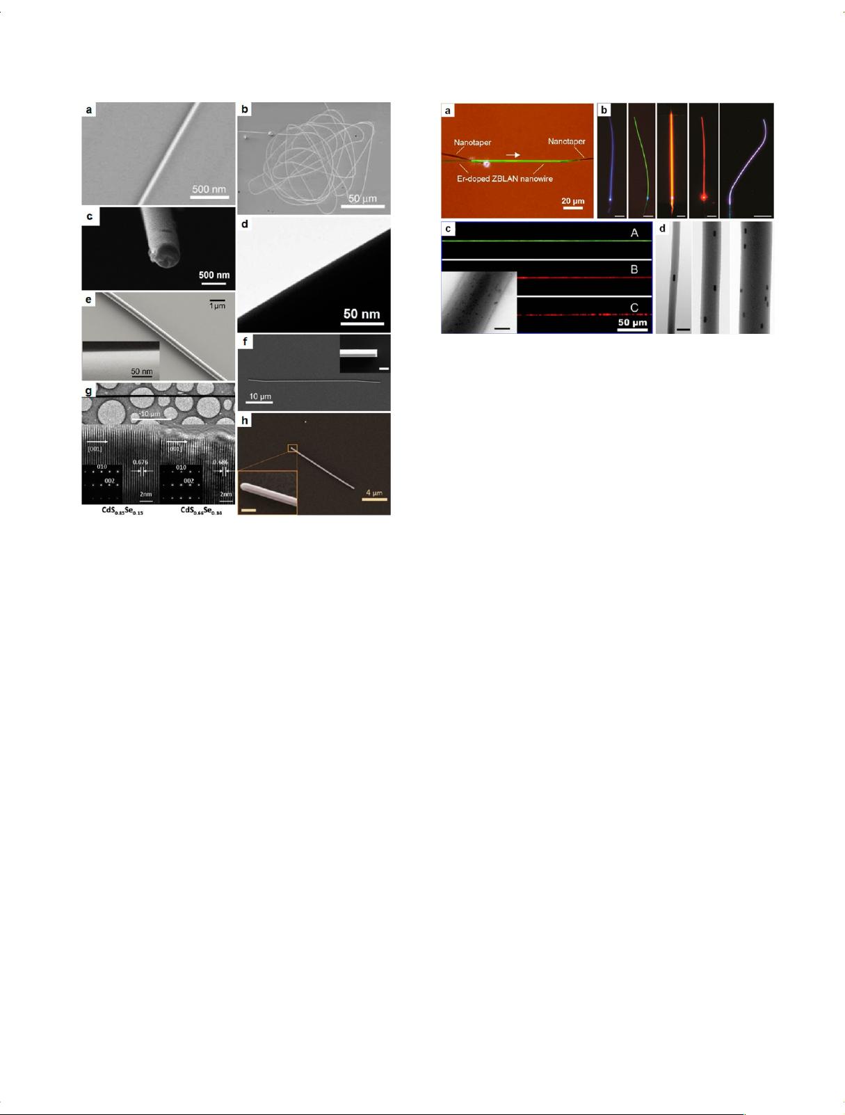
(Figure 1g)] and geometry (e.g., nanowire taper,
branch,
28
and comb
29
) of the semiconductor nanowire for
photonic applications. In addition, nanowires grown by the
bottom-up approach can be as thin as several nanometers,
providing an opportunity to manifest evident quantum
confinement effects
30
and modify photonic properties of
the nanowires for light absorption and emission.
Typical materials for optical-frequency plasmonic appli-
cations are noble metals such as Au and Ag. Despite the
high absorption, radiation loss originating from crystalline
boundary scattering cannot be neglected, and metal nano-
wires with good crystalline integrity is usually desired for
both localized and propagation surface plasmons.
31
Among
various fabrication methods, seed-growth method is
deemed the most successful technique for growing metal
nanowires with smooth sidewalls, large length, high yield,
and crystalline structures (Figure 1h).
32,33
Two or more materials can be combined into a complex
mixture for fabricating functionally activated photonic nano-
wires. Several approaches, including doping, blending,
coating, and near-field coupling, can be used to incorporate
exotic functional materials into nanowires. For example, by
doping the starting material before nanowire drawing, our
group incorporated a variety of functional dopants, includ-
ing rare-earth ions (Figure 2a),
15
dye molecules (Figure 2b),
18
QDs (Figure 2c),
34
and metal nanoparticles (Figure 2d),
35
into
photonic nanowires. Also, to functionalize the nanowire
FIGURE 2. Functionally doped photonic nanowires. (a) Photolumines-
cence (PL) image of a 320 nm diameter Er-doped ZBLAN
(53ZrF
4
20BaF
2
3.9LaF
3
3AlF
3
20NaF0.1ErF
3
) glass nanowire ex-
cited by a 975 nm wavelength light. Adapted from ref 15 with permis-
sion. Copyright 2006 Optical Society of America. (b) PL images of
photoexcited dye-molecule-doped polymer nanowires. Scale bars,
50 μm. Adapted from ref 18 with permission. Copyright 2010 American
Chemical Society. (c) PL images of PS nanowires doped with CdSe QDs
with different sizes. Inset, TEM image of a 280 nm diameter QD-doped
PS nanowire. Inset scale bar, 100 nm. Adapted from ref 34 with
permission. Copyright 2011 Wiley. (d) TEM images of Au-nanorod-
doped polyacrylamide (PAM) nanowires with diameters of 150, 360,
and 600 nm, respectively. Scale bar, 250 nm. Adapted from ref 35 with
permission. Copyright 2012 American Chemical Society.
FIGURE 1. Electron microscope images of some typical 1D photonic
nanowires. (a) A 50 nm diameter silica nanowire. Adapted from ref 13
with permission. Copyright 2003 Nature Publishing Group. (b) A 4 mm
length 260 nm diameter coiled silica nanowire. Adapted from ref 13
with permission. Copyright 2003 Nature Publishing Group. (c) Cross-
section of a 480 nm diameter silica nanowire. Adapted from ref 14 with
permission. Copyright 2008 Elsevier. (d) Sidewall of a 210 nm diameter
phosphate glass nanowire. Adapted from ref 15 with permission.
Copyright 2006 Optical Society of America. (e) A 400 nm diameter
polystyrene (PS) nanowire doped with rhodamine B (RhB). Adapted from
ref 18 with permission. Copyright 2010 American Chemical Society. (f) A
200 nm diameter CdSe nanowire. Adapted from ref 25 with permission.
Copyright 2011 American Chemical Society. (g) A CdSSe nanowire
(above) and its corresponding high-resolution transmission electron
microscopy (HRTEM) images and selected area electron diffraction
(SAED) patterns taken from several representative regions along its
length (below). Adapted from ref 27 with permission. Copyright 2011
American Chemical Society. (h) A 260 nm diameter Ag nanowire. Inset
scale bar, 400 nm. Adapted from ref 33 with permission. Copyright 2010
Optical Society of America.


