没有合适的资源?快使用搜索试试~ 我知道了~
首页PMW3360DM-T2QU:专业游戏导航芯片详细手册
PMW3360DM-T2QU:专业游戏导航芯片详细手册
需积分: 34 23 下载量 166 浏览量
更新于2024-07-16
1
收藏 2.5MB PDF 举报
PMW3360DM-T2QU是一款由PixArt Imaging Inc.开发的高端光学游戏导航芯片,专门针对专业游戏玩家的需求设计。该产品属于PMW3360系列,其V1.5版本的datasheet提供了详尽的寄存器说明,适用于该系列的其他类似传感器。此芯片集成了导航芯片和红外(IR) LED,采用16针塑封DIP封装,旨在提供卓越的游戏体验。 该芯片的特点包括: 1. 集成式设计:16针封装设计中内置了红外LED,简化了硬件布局,减少了外部组件的需求。 2. 工作电压范围:PMW3360DM-T2QU支持1.8V至2.1V的宽电压操作,适应各种电源环境。 3. 可选的抬升检测功能:为了增强精确度,芯片提供了手动抬升截止校准选项,允许用户根据实际应用调整对抬升动作的响应,提供2mm和3mm两种不同的抬升检测高度,以满足不同游戏场景下的需求。 4. 高速性能:芯片具有高达250英寸/秒(典型)的高精度运动检测速度和50g的最大加速度,确保快速反应和流畅的游戏体验。 5. 分辨率选择:支持高达12000cpm(每分钟线数)的可选分辨率,这使得它可以适应对细节捕捉有极高要求的游戏。 6. 自适应帧率算法:内置的可变帧率算法可以根据实际运动情况动态调整帧率,这对于无线游戏应用来说尤其重要,能够降低延迟,提升玩家的沉浸感。 PMW3360DM-T2QU是一款专为专业游戏市场设计的高性能光学导航芯片,它的核心优势在于其集成度、灵活性和高精度,为电子游戏设备制造商提供了强大的技术支持,以提升现代游戏控制器的性能和用户体验。开发者在使用这款芯片时,应仔细阅读datasheet上的详细信息,以充分利用其所有特性和优化设计。
资源详情
资源推荐
10
Version1.50|26Sep2016
PixArtImagingInc.Allrightsreserved.Anyportioninthispapershallnotbereproduced,copied,ortransformedtoany
otherforms
PixArtImagingInc.
PMW3360ProductDatasheet
OpticalGamingNavigationChip
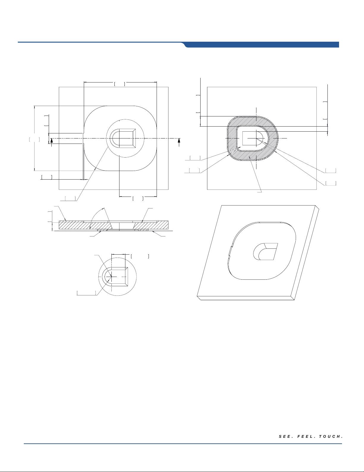
Figure8.RecommendedBasePlateOpening
Note:MousefeetshouldbeplacedclosetotheopeningtostabilizethesurfacewithintheFOVofthechip.
21.35
0.841
19.00
0.748
10.97
0.432
3.00
0.118
4X
R7.05
0.278
0.25
0.010
C C
F
68.50°
2.40
0.094
Navigation Surface
Base Plate
Lens Sitting Plane
SECTION C-C
Surrounding Mouse Feet
4.00 min.
0.158 min.
R2.00 max.
0.079 max.
DETAIL F
SCALE 5 : 1
Optical Center
3.00 min.
0.118 min.
All Around
1.50 min.
0.059 min.
All Around
2X
R1.00
0.039
2X
R4.00
0.157
R3.50
0.138
R6.50
0.256
Surrounding Mouse Feet
11
Version1.50|26Sep2016
PixArtImagingInc.Allrightsreserved.Anyportioninthispapershallnotbereproduced,copied,ortransformedtoany
otherforms
PixArtImagingInc.
PMW3360ProductDatasheet
OpticalGamingNavigationChip
1.4 PCBAssemblyRecommendation
1) InserttheintegratedchipandallotherelectricalcomponentsintoPCB.
2)
Wave‐soldertheentireassemblyinano‐washsolderprocessutilizingsolder‐fixture.Asolder‐fixtureisrequiredto
protectthechipfromfluxsprayandwavesolder.
3)
Avoidgettinganysolderfluxontothechipbodyasthereispotentialforfluxtoseepintothechippackage,thesolder
fixtureshouldbedesignedtoexposeonlythechipleadstofluxspray&moltensolderwhileshieldingthechipbody
andopticalapertures.Thefixtureshouldalsose
tthechipatthecorrectpositionandheightonthePCB.
4)
Placethelensontothebaseplate.Caremustbetakentoavoidcontaminationontheopticalsurfaces.
5)
Removetheprotectivekaptontapesfromopticalaperturesofthechip.CaremustbetakentopreventContaminants
fromenteringtheapertures.DonotplacethePCBwiththechipfacingupduringtheentiremouseassemblyprocess.
HoldthePCBverticallywhenremovingkaptontape.
6)
InsertPCBassemblyoverthelensontothebaseplatealigningposttoretainPCBassembly.Thechippackagewillself‐
aligntothelensviatheguideposts.TheopticalpositionreferenceforthePCBissetbythebaseplateandlens.Note
thatthePCBmotionduetobu
ttonpressesmustbeminimizedtomaintainopticalalignment.
7)
Recommendation:Thelenscanbepermanentlysecuredtothechippackagebymeltingthelens’guidepostsoverthe
chipwithheatstakingprocess.PleaserefertotheapplicationnotePMS0122‐LM19‐LSI‐ANformoredetails.
8)
Installmousetopcase.TheremustbeafeatureinthetopcasetopressdownontothePCBassemblytoensureall
componentsarestackedorinterlockedtothecorrectvertical height.
ChipBlockDiagram
Fi
gure9.BlockdiagramofPMW3360DM‐T2QU
SERIALCOMMUNICATION
PICTURE
ELEMENTARR AY
NCS
SCLK
MO TION
MO SI
PMW3360DM‐T2QU
DSP
OSCILLATOR
LED
DRI VE
PO W ERANDCONTROL
VDDO
VDD
GND
MI SO
NRESET
VDDPIX
NC
LED_P
NC
LED
NC
NC
12
Version1.50|26Sep2016
PixArtImagingInc.Allrightsreserved.Anyportioninthispapershallnotbereproduced,copied,ortransformedtoany
otherforms
PixArtImagingInc.
PMW3360ProductDatasheet
OpticalGamingNavigationChip
1.5 ReferenceSchematics
Figure10.Schematicdiagramforinterfa ce betweenPMW3360DM ‐T2QUandmicrocontrolleronawiredsolution
V+
1
DATA-
2
DATA+
3
ID
4
GND
5
SHIELD
0
CON1
USB_MINIB_5P
R1
0R
1
TP3
R3
33R
R4
33R
D-
D+
R2
1.5k
USB_SW
C1
10uF
C2
100nF
R5
0R
USB_5V
1
TP1
1 2
3 4
5 6
J1
PCB_SOCKET_1.27MM_2X3P
SWDIO
RESETSWCLK
SWO
1
TP5
1
TP7
1
TP6
1
TP8
Serial Wire Debug
USB Input
COM
3
B
2
A
1
Q1
Z-Encoder
ZB
ZA
1
3
2
SW1
Left Click
1
3
2
SW2
Right Click
1
3
2
SW3
Middle Click
C28
100nF
C27
100nF
R25
10k
R23
10k
VDD_3.3V VDD_3.3V
LEFT RIGHT MIDDLE
R27
10k
VDD_3.3V
C29
100nF
1
3
2
SW4
CPI+ Button
CPI+
R24
10k
VDD_3.3V
C32
100nF
1
3
2
SW5
CPI- Button
CPI-
R26
10k
VDD_3.3V
C33
100nF
Switches
D1
YLW
R28
470R
D2
YLW
R29
470R
D3
YLW
R30
470R
VDD_3.3V
CPI_LED1
CPI_LED2
CPI_LED3
CPI Indicator
RESET
3
PIO0_1
4
PIO1_19/DTR/SSEL1
2
TDI/PIO0_11
32
PIO0_22/MISO1
30
SWCLK/PIO0_10/SCK0
29
PIO0_9/MOSI0
28
PIO0_8/MISO0
27
PIO1_25
1
XTALOUT
7
VDD
8
PIO1_21/DCD/MISO1
26
PIO1_28/SCLK
24
PIO0_7/CTS
23
PIO0_6/USB_CONNECT/SCK0
22
PIO1_24
21
USB_DP
20
USB_DM
19
PIO1_31
25
PIO1_23/SSEL1
18
PIO0_21/MOSI1
17
PIO0_5/SDA
16
XTALIN
6
VSS
5
PIO0_20
9
PIO0_2/SSEL0
10
PIO1_26/RXD
11
PIO1_27/TXD
12
PIO1_20/DSR/SCK1
13
PIO0_3/USB_VBUS
14
PIO0_4/SCL
15
PIO0_16/WAKEUP
40
SWDIO/PIO0_15
39
PIO1_22/RI/MOSI1
38
PIO1_14/DSR/RXD
37
PIO1_13/DTR
36
TRST/PIO0_14
35
TMS/PIO0_12
33
PIO1_29/SCK0
31
TDO/PIO0_13
34
VSS
41
PIO0_23
42
PIO1_15/DCD/SCK1
43
VDD
44
PIO0_17/RTS/SCLK
45
PIO0_18/RXD
46
PIO0_19/TXD
47
PIO1_16/RI
48
U3
LPC11U34FBD48/311
C31
18pF
VDD1_3.3V
CPI+
CPI-
MISO
MOSI
SCLK
NCS
LEFT
RIGHT
MIDDLE
ZA
ZB
D-
D+
C30
18pF
MOTION
MCU Part
13
2
4
X1
12MHz
CPI_LED1
CPI_LED2
CPI_LED3
SWCLK
SWDIOUSB_CON
USB_5V
RESET
SN_NRESET
SW_1
SW_2
VDD2_3.3V
XTAL_OUT
XTAL_IN
XTAL_OUT
XTAL_IN
OSC
USB Switch
c
3
b
1
e
2
Q2
MMBT3906LT1
VDD_3.3V
R7
10k
R6
2.2k
USB_CON
USB_SW
R11
0R
C5
10uF
C8
100nF
VDD1_3.3V
R12
0R
C6
10uF
C9
100nF
VDD2_3.3V
R13
0R
C7
10uF
C10
100nF
VDD3_3.3V
R22
0R
C23
10uF
C24
100nF
VDD4_3.3V
VDD_3.3V
C11
10uF
C13
100nF
VDD5_SS
C12
10uF
C14
100nF
VDD6_SS
VDD_SS
21
J2
PH_2.54MM_1X2P
21
J3
PH_2.54MM_1X2P
JP2
JP3
C25
10uF
C26
100nF
USB_5V
Capacitor Filter
d
3
s
2
g
1
Q3
BSS223PWH6327XTSA1
SW_1
R8
20R
VDD5_SS
LED1_P
d
3
s
2
g
1
Q4
BSS223PWH6327XTSA1
SW_2
R9
39R
VDD5_SS
LED1_P
LED Switches
1
NC
2
VDDPIX
3
6
VDD
4
VDDIO
5
LED_P
15
NC
14
NCS
13
MISO
12
MOSI
11
SCLK
10
MOTION
9
NRESET
7
NC
16
GND
8
U6
PWM3360DM-T2QU
R10
10k
MISO
M
OSI
VDD6_SS
SCLK
NCS
MOTION
VDD_3.3V
LED_P
NRESET
1
TP9
1
TP17
1
TP16
1
TP15
1
TP12
Insert RCPT 1.02MM
PCB1
1
Placement at Top Layer
IN
1
EN
3
FB
4
GND
2
OUT
5
U1
TPS73601DBVR
C17
1uF
C15
100nF
USB_5V
C21
10uF
C19
100nF
R14
52.3k
R16
30.1k
R17
0R
1
TP2
VDD_3.3V
IN
1
EN
3
FB
4
GND
2
OUT
5
U2
TPS73601DBVR
C18
1uF
C16
100nF
USB_5V
C22
10uF
C20
100nF
R18
56k
R21
0R
1
TP2
VDD_SS
R15
37.4k
2.0V
1.9V
1.8V
LDO
1
2
3
SW6
SLIDE SW SPDT
GND OPEN
R19
63.4k
R20
75k
21
J4
PH_2MM_1X2P
21
J5
PH_2MM_1X2P
21
J6
PH_2MM_1X2P
JP4
JP5
JP6
AGND
USB_5V
NRESET
MISO
MOSI
SCLK
MOTION
SWCLK
SWO
SWDIO
RESET
VCC_3.3V
VCC_SS
PCB2
2
Slide Switch place bottom.
PCB3
3
Default
MCU FLASH OPT
1
Default Setting
J5 Short by JP5 (1.9V)
NC
NC
C3
4.7uF/10V
C4
100nF
VDD6_SSVDD4_3.3V
Chip pin 1 facing down
Chip ůŽĐŬ
剩余56页未读,继续阅读
MengXP
- 粉丝: 152
- 资源: 60
上传资源 快速赚钱
- 我的内容管理 展开
- 我的资源 快来上传第一个资源
- 我的收益 登录查看自己的收益
- 我的积分 登录查看自己的积分
- 我的C币 登录后查看C币余额
- 我的收藏
- 我的下载
- 下载帮助
最新资源
- C++多态实现机制详解:虚函数与早期绑定
- Java多线程与异常处理详解
- 校园导游系统:无向图实现最短路径探索
- SQL2005彻底删除指南:避免重装失败
- GTD时间管理法:提升效率与组织生活的关键
- Python进制转换全攻略:从10进制到16进制
- 商丘物流业区位优势探究:发展战略与机遇
- C语言实训:简单计算器程序设计
- Oracle SQL命令大全:用户管理、权限操作与查询
- Struts2配置详解与示例
- C#编程规范与最佳实践
- C语言面试常见问题解析
- 超声波测距技术详解:电路与程序设计
- 反激开关电源设计:UC3844与TL431优化稳压
- Cisco路由器配置全攻略
- SQLServer 2005 CTE递归教程:创建员工层级结构
资源上传下载、课程学习等过程中有任何疑问或建议,欢迎提出宝贵意见哦~我们会及时处理!
点击此处反馈
安全验证
文档复制为VIP权益,开通VIP直接复制
信息提交成功