
www.ti.com
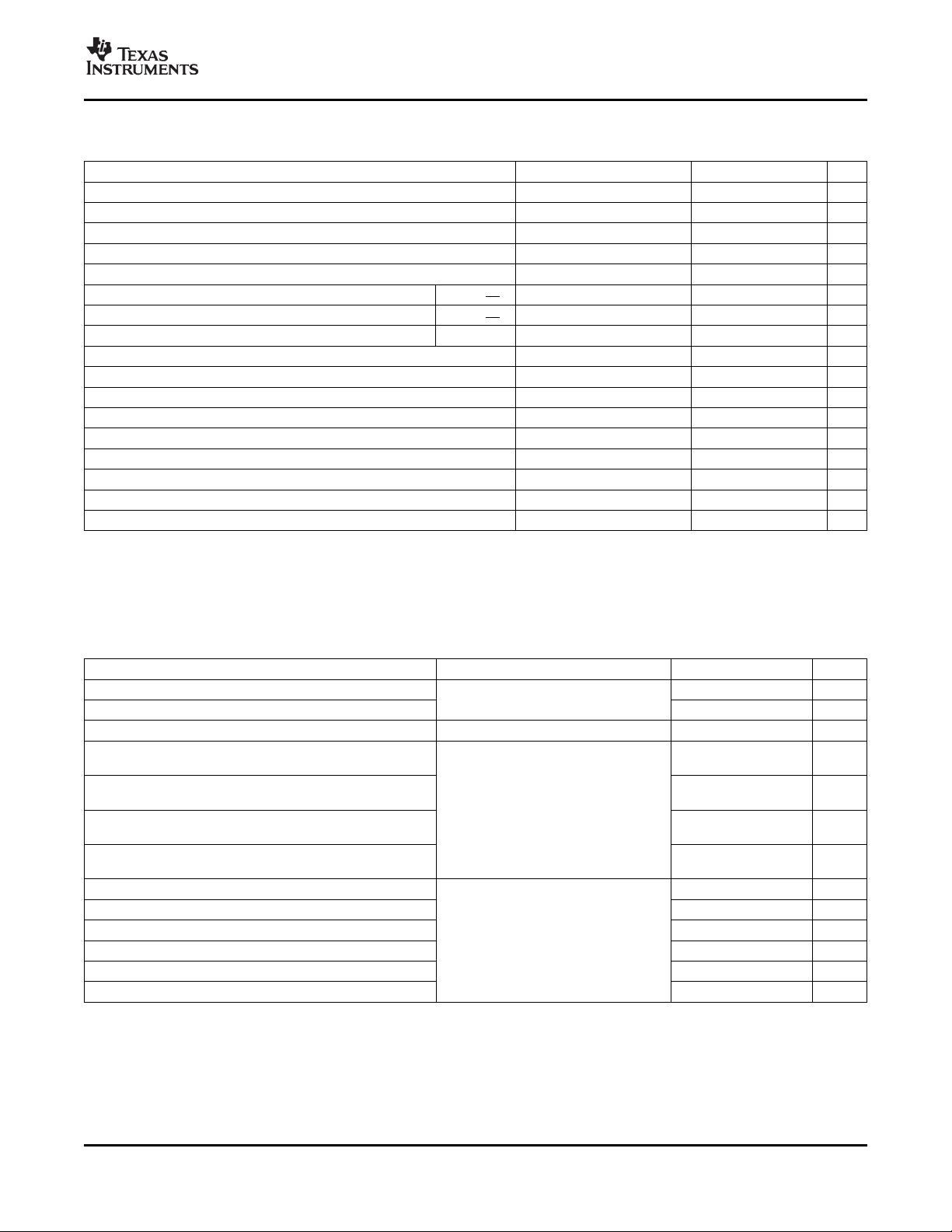
RECEIVER ELECTRICAL CHARACTERISTICS
DRIVER SWITCHING CHARACTERISTICS
TB5T1
SLLS589C – NOVEMBER 2003 – REVISED OCTOBER 2007
over operating free-air temperature range unless otherwise noted
PARAMETER TEST CONDITIONS MIN TYP MAX UNIT
V
OL
Output low voltage V
CC
= 4.5 V, I
OL
= 8.0 mA 0.4 V
V
OH
Output high voltage V
CC
= 4.5 V, I
OH
= -400 µA 2.4 V
V
IL
Enable input low voltage
(1)
V
CC
= 5.5 V 0.8 V
V
IH
Enable input high voltage
(1)
V
CC
= 4.5 V 2 V
V
IK
Enable input clamp voltage V
CC
= 4.5 V, I
I
= -5 mA -1
(2)
V
V
TH+
Positive-going differential input threshold voltage
(1)
|V
Rin
- V
Rin
| n = 1 or 2 100 mV
V
TH-
Negative-going differential input threshold voltage
(1)
|V
Rin
- V
Rin
| n = 1 or 2 -100
(2)
mV
V
HYST
Differential input threshold voltage hysteresis (V
TH+
- V
TH-
) 50 mV
I
OZL
Off-state output low current (high Z) V
CC
= 5.5 V, V
O
= 0.4 V -20
(2)
µA
I
OZH
Off-state output high current (high Z) V
CC
= 5.5 V, V
O
= 2.4 V 20 µA
I
OS
Short circuit output current
(3)
V
CC
= 5.5 V -100
(2)
mA
I
IL
Enable input low current V
CC
= 5.5 V, V
IN
= 0.4 V -400
(2)
µA
I
IH
Enable input high current V
CC
= 5.5 V, V
IN
= 2.7 V 20 µA
I
IH
Enable input reverse current V
CC
= 5.5 V, V
IN
= 5.5 V 100 µA
II
L
Differential input low current V
CC
= 5.5V, V
IN
= -1.2 V -2
(2)
mA
I
IH
Differential input high current V
CC
= 5.5V, V
IN
= 7.2 V 1 mA
R
O
Output resistance 20 Ω
(1) The input levels and difference voltage provide no noise immunity and should be tested only in a static, noise-free environment.
(2) This parameter is listed using a magnitude and polarity/direction convention, rather than an algebraic convention, to match the original
Agere data sheet.
(3) Test must be performed one lead at a time to prevent damage to the device.
over operating free-air temperature range unless otherwise noted
PARAMETER TEST CONDITIONS MIN TYP MAX UNIT
t
P1
Propagation delay time, input high to output
(1)
C
L
= 5 pF, See Figure 2 and Figure 6 1.2 2 ns
t
P2
Propagation delay time, input low to output
(1)
1.2 2 ns
Δ t
P
Capacitive delay 0.01 0.03 ns/pF
t
PHZ
Propagation delay time, C
L
= 5 pF, See Figure 3 and Figure 6 8 12 ns
high-level-to-high-impedance output
t
PLZ
Propagation delay time, 7 12 ns
low-level-to-high-impedance output
t
PZH
Propagation delay time, 4 12 ns
high-impedance-to-high-level output
t
PZL
Propagation delay time, 5 12 ns
high-impedance-to-low-level output
t
skew1
Output skew, |t
P1
- t
P2
| C
L
= 5 pF, See Figure 2 andFigure 6 0.15 0.3 ns
t
skew2
Output skew, |t
PHH
- t
PHL
|, |t
PLH
- t
PLL
| 0.15 1.1 ns
t
skew(pp)
Part-to-part skew
(2)
0.1 1 ns
Δ t
skew
Output skew, difference between drivers 0.3 ns
t
TLH
Rise time (20%-80%) 0.7 2 ns
t
THL
Fall time (80%-20%) 0.7 2 ns
(1) Parameters t
P1
and t
P2
are measured from the 1.5 V point of the input to the crossover point of the outputs (see Figure 2 ).
(2) t
skew(pp)
is the magnitude of the difference in propagation delay times between any specified outputs of two devices when both devices
operate with the same supply voltage, at the same temperature, and have identical packages and test circuits.
Copyright © 2003 – 2007, Texas Instruments Incorporated Submit Documentation Feedback 5
Product Folder Link(s): TB5T1
剩余21页未读,继续阅读


